Exploring the Efficiency of 3D-Stacked AI Chip Architecture for LLM Inference with Voxel
Abstract: To overcome the well-known memory bottleneck of AI chips, 3D stacked architectures that employ advanced packaging technology with high-density through-silicon vias (TSVs) pins have proven to be a promising solution. The 3D-stacked AI chip enables ultra-high memory bandwidth between compute and memory by stacking numerous DRAM banks atop many AI cores in a distributed manner. However, it is not easy to explore the efficiency of the 3D-stacked AI chip, due to its unique distributed nature. And we need to carefully consider multiple intertwined factors that range from upper-level computing paradigm to ML compiler optimizations, and to the underlying hardware architecture. In this paper, we develop Voxel, a fast and compiler-aware end-to-end simulation framework to facilitate exploring the efficiency of 3D-stacked AI chips for LLM inference. Voxel enables the software/hardware co-exploration by employing a programming interface that allows ML compilers to customize the model execution plans. After validating the results of Voxel with an emulator on real silicon, we thoroughly examine the impact and correlation of different aspects of 3D-stacked AI chips, including state-of-the-art compute paradigms, tile-to-core mapping, tensor-to-bank mapping, NoC topologies and link bandwidth, DRAM bank bandwidth, per-core SRAM capacity, and energy/thermal constraints. Our findings disclose that the end-to-end efficiency of a 3D stacked AI chip not only is determined by the cooperative function of these factors, but also significantly depends on the mappings from tiles to AI core and DRAM banks. We report our findings throughout the paper, with the expectation that they will shed light on the development of the 3D-stacked AI chip ecosystem. We will open source Voxel and our study results for public research.

Paper Prompts
Sign up for free to create and run prompts on this paper using GPT-5.
Top Community Prompts
Explain it Like I'm 14
What this paper is about
This paper looks at a new kind of computer chip designed for AI, called a 3D‑stacked AI chip. These chips put memory on top of the parts that do the calculations, like building a multi‑story library right above the classrooms so students can grab books quickly. The goal is to make running LLMs faster and more efficient.
To study how well these chips could work, the authors built a special simulator called VoxelSim. It lets them test different software strategies and hardware designs together, so they can see what really helps speed and efficiency.
The big questions the paper asks
The paper focuses on simple, practical questions:
- How do we organize work on a 3D‑stacked AI chip so it runs LLMs quickly?
- Which software choices (like how we split tasks) and hardware choices (like how memory and cores are connected) matter most?
- How can we test all these choices without needing a physical chip that doesn’t exist yet?
How they did the research (in everyday terms)
Think of an AI chip as a city:
- Cores are workers in buildings doing math.
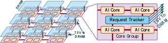
- Memory (DRAM banks) are rooms full of books stacked above the workers.
- The Network‑on‑Chip (NoC) is the road system between buildings.
- SRAM is each worker’s desk where they keep the papers they’re using right now.
- TSVs (through‑silicon vias) are like elevator cables that connect floors directly, making it fast to grab books from above.
Here’s the approach:
- They built VoxelSim, a computer program that simulates this city. It’s “compiler‑aware,” meaning it listens to the software that plans the workers’ tasks and routes, instead of guessing.
- The simulator represents tasks as events (compute, move data, sync). It then plays out these events across the cores, memory banks, and roads, step by step.
- To keep the simulation fast, it spots repeating memory access patterns (like reusing a recipe over and over) and reuses the timing results instead of recalculating everything. This speeds up work without losing accuracy.
- It also checks heat limits (thermal constraints). If too much power is used in a small area, it slows things down—like a game console that throttles to avoid overheating.
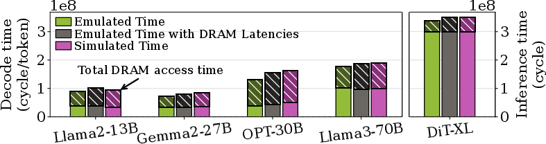
- Because there aren’t real 3D‑stacked AI chips on the market yet, they validated VoxelSim using a real AI chip (Graphcore IPU) as an emulator. The results from VoxelSim were very close—within about 0.24% to 6.8%—to the emulated hardware measurements.
What they found and why it matters
Here are the main results, introduced to highlight what improves speed and efficiency:
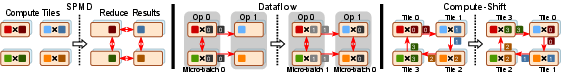
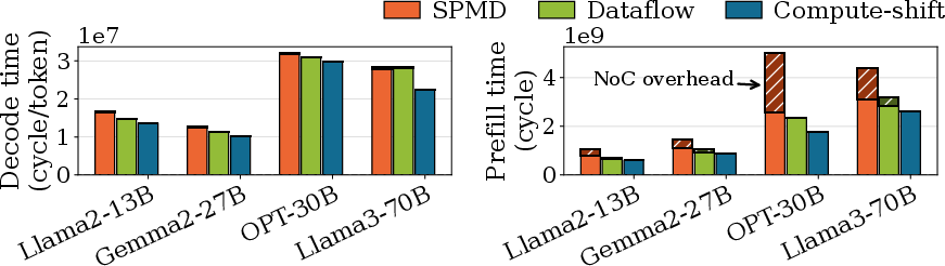
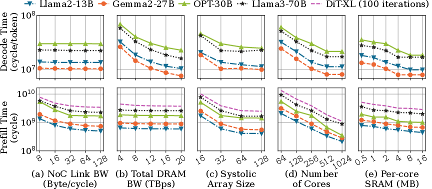
- Different ways of organizing work (“compute paradigms”) matter a lot. The best strategy they tested, called compute‑shift, overlaps computation, memory access, and communication, and can be up to 1.84× faster than others. Translation: plan so workers can compute while data is moving, not waiting around.
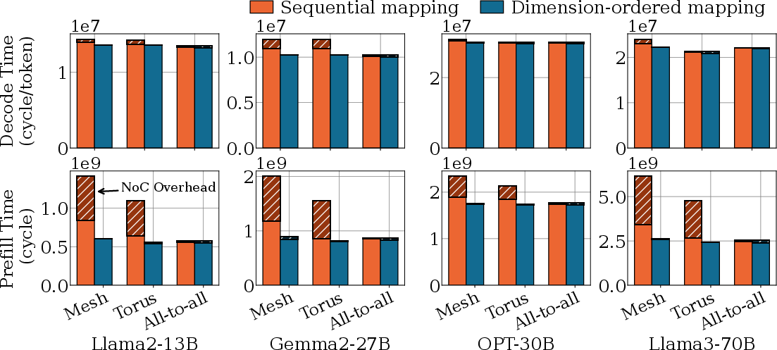
- Mapping tiles (small pieces of a big task) to cores smartly reduces traffic. A “dimension‑ordered” mapping (placing related tasks near each other in a grid) minimizes the number of road hops on the NoC. With a simple 2D mesh road system, this mapping gives near‑optimal performance.
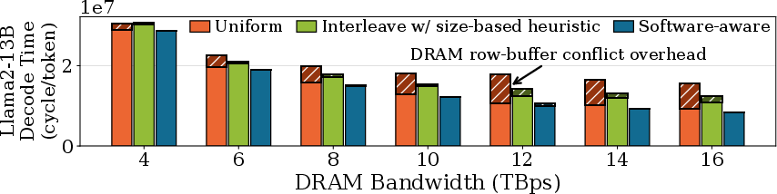
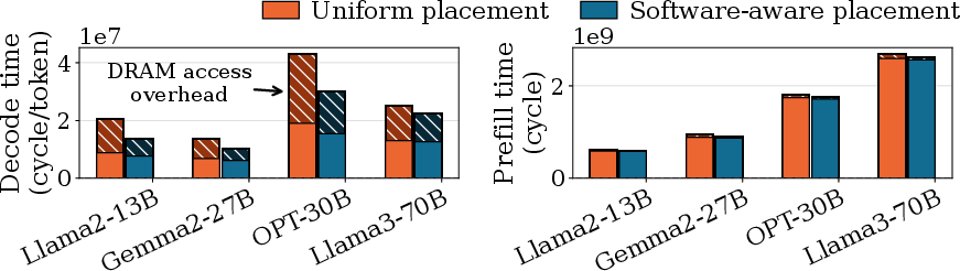
- Placing parts of tensors (big arrays of numbers) in the right memory banks reduces slowdowns. If you place them carelessly (uniformly), the chip keeps switching between rows in memory (row‑buffer conflicts), which stalls the dedicated memory buses. A software‑aware placement strategy can cut this overhead by up to 80.7%.
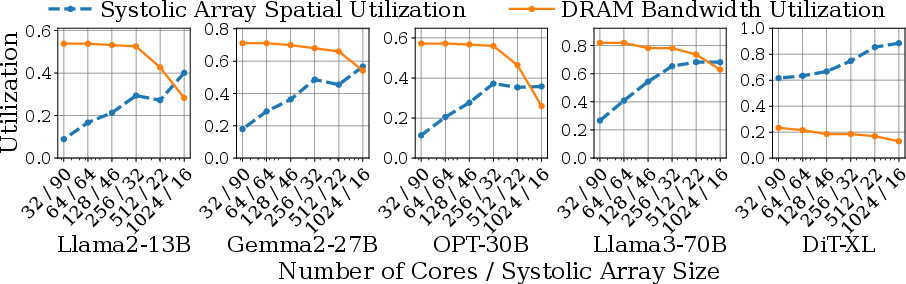
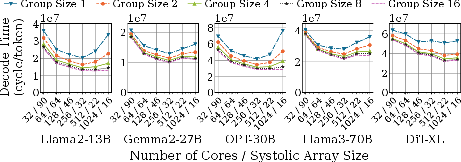
- Adding more cores isn’t always good. More workers can cause more memory row conflicts if they aren’t coordinated. Grouping nearby cores and synchronizing their DRAM accesses (using a hardware tracker) improves both core and memory use.
- SRAM (the desk space per worker) helps mostly in memory‑bound phases like LLM decoding (when you generate tokens one by one). Larger SRAM lets the core prefetch more data and go faster—until memory bandwidth is saturated. In compute/communication‑bound phases like LLM prefill (the initial big matrix crunch), bigger SRAM brings limited gains because cores are already very busy.
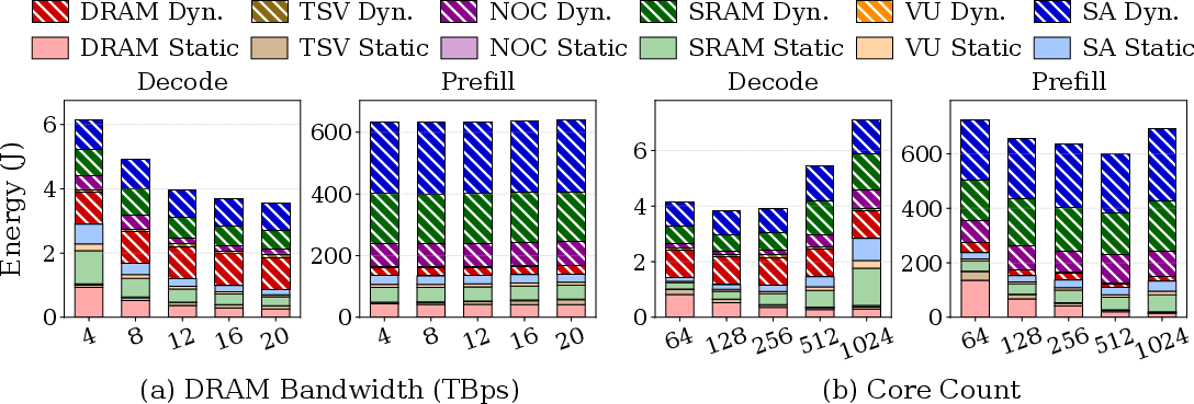
- Energy efficiency behaves differently for different workloads. For memory‑bound tasks, increasing DRAM bandwidth speeds things up and saves energy overall (less time running). For compute‑bound tasks, just adding more cores may not save energy: it increases power without giving enough performance boost.
Why this matters for the future
This research shows that to get the most out of 3D‑stacked AI chips, you need to design software and hardware together:
- Software should plan where data lives and how tasks move, so memory buses stay busy and roads don’t get clogged.
- Hardware should provide the right mix of cores, local SRAM, NoC topology, and DRAM bandwidth, tuned for real LLM workloads.
- The simulator (VoxelSim) gives designers and researchers a way to explore these choices quickly and reliably before building actual chips.
If these ideas guide future chips, we could see faster, more energy‑efficient LLMs that respond quicker and cost less to run. The authors plan to open‑source VoxelSim, which means many people can use it to design better AI hardware and software.
Knowledge Gaps
Knowledge gaps, limitations, and open questions
Below is a concise list of unresolved issues that future work could directly act on:
- Lack of validation on true 3D-stacked AI silicon: results are cross-validated via an IPU-based emulator (SRAM-backed) with DRAM latencies replayed offline. Missing are end-to-end couplings among DRAM, NoC, TSVs, and thermal effects present in real 3D stacks. What changes when validated on actual 3D-stacked devices?
- Simplified thermal model: a static power-density cap and linear frequency scaling are used, with no spatial–temporal heat flow, vertical thermal coupling across stacks, hotspots, or dynamic cooling/thermal throttling policies. How do conclusions change under realistic thermal networks and temperature-dependent behavior?
- Temperature-dependent DRAM behavior omitted: DRAM refresh rates and timing parameters (and their performance impact) are not modeled as a function of temperature. How significant are the performance/energy shifts under realistic thermal DRAM models?
- NoC macromodeling only: link sharing is modeled by hop count and bandwidth; router microarchitecture (buffers, VCs, arbitration), flit-level contention, adaptivity, backpressure, serialization latency, packetization, and DMA endpoints are abstracted. How sensitive are findings to cycle-accurate NoC designs and alternative routing/flow control?
- Restrictive NoC assumption: “NoC bandwidth is strictly lower than SRAM read bandwidth” is assumed for core-to-core communication. This constrains the design space; what happens when NoC is provisioned at or above SRAM rates?
- Limited NoC topology exploration: only 2D mesh, torus, and all-to-all are considered; no hierarchical, 3D vertical, or reconfigurable/hybrid NoCs. Which topologies and routing algorithms best co-design with compute-shift and collective algorithms?
- DRAM model gaps despite Ramulator integration: simplified refresh handling (arrival shifting), limited treatment of read/write turnarounds, bank-group/pseudo-channel effects, on-die ECC, power-down states, tFAW and bus turnaround penalties, and temperature dependence. How do these factors alter row-buffer conflict rates and tensor-to-bank placement efficacy?
- Address mapping policy underexplored: the bank/row/column bit-slicing (and interleaving) is crucial to row-buffer locality yet is not described or co-optimized with tensor layouts. Which mapping policies minimize conflicts across LLM operators?
- TSV/interconnect physics omitted: no modeling of TSV electrical parasitics, driver power, latency, crosstalk, keep-out zones (KOZ), yield, or area routing constraints. What TSV pitch/width/bus-count trade-offs optimize performance/energy/area under realistic constraints?
- “Core group” tracker lacks microarchitectural specification: area/power timing overhead, protocol, deadlock/fairness, DRAM scheduling interaction, NoC traffic side effects, and scalability with heterogeneous workloads remain unspecified. What are the concrete design and cost/benefit?
- Compiler automation missing: VoxelSim exposes an interface, but there is no auto-scheduler/cost model that searches tilings, tile-to-core, and tensor-to-bank mappings. How can compilers automatically learn and generalize these mappings across models and hardware?
- Software-aware tensor-to-bank placement unspecified: the strategy is referenced but not detailed (objective, constraints, algorithm), nor its runtime overheads or portability across access patterns (e.g., fused ops, varying batch/sequence lengths). What concrete algorithms achieve these gains robustly?
- Compute–communication overlap realism: overlap relies on assumptions about DMA engines, outstanding request limits, and scheduling; these are not modeled. What hardware/software support is required to realize the reported overlaps under realistic queues and dependencies?
- Memory hierarchy simplifications: only per-core scratchpad SRAM is modeled; there is no cache/coherence, remote-SRAM consistency protocol, or barriers’ overhead characterization. How do coherence or explicit synchronization costs affect end-to-end performance?
- Prefetching and scheduling policy gaps: mvdata events are created on demand; there is no modeling of hardware/software prefetchers, DMA queue prioritization, reordering, or throttling policies. What is the achievable prefetch window and hit-rate in practice?
- Workload scope limited to LLM inference: no training, Mixture-of-Experts (routing skew), retrieval-augmented models, sparse/irregular kernels, or non-LLM workloads (vision/graph). Do conclusions (e.g., on compute-shift and mappings) generalize?
- Latency-centric inference not analyzed: focus is on throughput; token-by-token decode SLOs, tail-latency under contention, and dynamic batching are not studied. What are the latency/throughput trade-offs and scheduling policies under 3D constraints?
- KV-cache and attention specifics underexplored: placement/replication/eviction of KV caches, attention’s irregular accesses, and cross-token reuse impacts on bank conflicts and NoC traffic are not characterized.
- Quantization and precision diversity missing: only BF16 is modeled; effects of FP8/INT8/INT4, mixed precision, and sparsity/compression on DRAM bandwidth, row-buffer locality, and SRAM footprint are not evaluated.
- Energy/power model limitations: component models are stitched but not co-validated; leakage, temperature dependence, DVFS domains, power-gating transitions, clock/power distribution losses, TSV driver power, and refresh energy are not captured. How robust are the energy conclusions under realistic power management?
- Physical design constraints not enforced: floorplanning, clock trees, PDN/IR drop, routing congestion, TSV KOZ, and timing closure constraints may invalidate proposed mappings. How to integrate layout-aware constraints into mapping and topology choices?
- Collective communication modeling abstract: compound ops exist but algorithmic variants (ring/tree/butterfly), synchronization costs, and topology-aware algorithm selection are not explored. Which collectives best match 3D NoCs and compute-shift?
- Multi-chip scaling unaddressed: extending to multi-die packages or chip-to-chip fabrics (NVLink/BoW/UCIe), memory disaggregation, and their co-design with 3D stacking are open. How do mappings and compute paradigms adapt across chips?
- Reliability/yield concerns absent: TSV/DRAM faults, spare rows/TSVs, ECC overhead/performance, thermal-induced failures, and soft error rates are not modeled. What is the performance/energy cost of resilience in 3D-stacked AI chips?
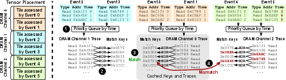
- Simulation technique robustness: the match-key DRAM trace coalescing assumes repetitive patterns; its correctness/speed on irregular or sparse access (e.g., MoE gating, retrieval) is not evaluated. What are fallback strategies and performance in worst-case traces?
- Parameter realism and sensitivity: defaults such as identical 1.6 GHz core/DRAM clocks, specific DRAM timing, and bank counts may not match HBM3/3E devices. A systematic sensitivity sweep against technology nodes and HBM generations is missing.
- Metrics beyond perf/energy: area efficiency (TOPS/mm²), cost, and process variability/binned SKUs are absent. Which design points dominate under realistic cost/area/thermal envelopes?
- Open-source artifact availability: the framework “will be open sourced,” but exact configs, traces, and scripts to reproduce figures are not yet available. What steps ensure reproducibility and external validation?
Practical Applications
Immediate Applications
The following applications can be executed with current tools, hardware, and workflows, leveraging VoxelSim’s methods, validated findings, and software–hardware co-design interface.
- VoxelSim-in-the-loop hardware/software co-design for AI accelerators
- Sectors: semiconductors, EDA, cloud hardware planning, hyperscalers
- What: Use VoxelSim to rapidly evaluate compute paradigms (e.g., compute-shift), tile-to-core mappings, tensor-to-bank placements, NoC topologies/bandwidth, core counts, and SRAM sizes for LLM inference designs and cluster deployment planning.
- Outputs: Design space exploration workflows; parametric performance/cost/energy dashboards; SKU selection guidance.
- Dependencies/assumptions: Access to VoxelSim; baseline LLM workloads and traces; calibration for specific DRAM timings and NoC parameters; acceptance of ~0.2–6.8% simulation error validated against IPU.
- Compiler passes for compute-shift scheduling and communication overlap
- Sectors: software tooling (XLA/MLIR/TVM), AI frameworks, cloud inference runtime
- What: Implement VoxelSim’s interface to express compute-shift plans that maximize overlap of compute, NoC communication, and DRAM accesses (shown to deliver up to 1.84× improvement over alternatives).
- Outputs: MLIR/XLA/TVM passes; runtime schedulers that hide memory latency in LLM prefill/decode.
- Dependencies/assumptions: Compiler support for tiling and collective ops; hardware support for prefetch and collective overlap; accurate workload phase detection (prefill vs decode).
- Dimension-ordered tile-to-core mapping on mesh/tiled NoCs
- Sectors: accelerator vendors, compiler teams, HPC scheduling
- What: Adopt dimension-ordered tile placement to minimize NoC hops and contention; aligns with finding that mesh with dimension-ordered mapping is near-optimal.
- Outputs: Compiler mapping heuristics; placement policies in deployment toolchains.
- Dependencies/assumptions: Knowledge of physical core topology; ability to pin tiles to specific cores; NoC bandwidth profiles.
- Software-aware tensor-to-DRAM bank placement to reduce row-buffer conflicts
- Sectors: compilers/runtimes, firmware, memory system software
- What: Introduce bank-aware memory planners that co-locate or separate tensors based on concurrent access patterns (up to 80.7% overhead reduction over uniform placement).
- Outputs: Memory allocation policies in compilers/runtimes; bank-conflict profilers; bank-aware tensor layout manifests.
- Dependencies/assumptions: Ability to influence bank/pseudo-channel mapping (vendor APIs, firmware hooks); knowledge of bank geometry; access pattern profiling.
- “Core grouping” via software coordination to mitigate DRAM conflicts
- Sectors: cloud inference runtimes, accelerator firmware
- What: Group physically adjacent cores and synchronize DRAM access epochs to reduce interleaved bank row switches (software emulation of the paper’s proposed hardware tracker).
- Outputs: Group-aware barriers; phased prefetch schedules; reduced bank thrash during shared-tensor reads.
- Dependencies/assumptions: Barrier/synchronization primitives; slight parallelism tradeoffs; hardware timers/counters for alignment; hardware tracker would provide further gains (see long-term).
- Energy-aware resource allocation based on workload phase
- Sectors: cloud operations, capacity planning, SRE
- What: Apply paper’s insight: increase DRAM bandwidth for memory-bound decode, but avoid over-scaling cores for compute-bound prefill where returns diminish.
- Outputs: Workload-aware autoscaling; instance type selection; cost-per-token optimizers.
- Dependencies/assumptions: Telemetry to classify phases; accurate per-phase utilization models; DRAM bandwidth configurability (e.g., channel activation policies).
- Integrate DRAM-trace coalescing into memory simulation workflows
- Sectors: EDA, academic simulation tooling
- What: Reuse VoxelSim’s “match key” technique to accelerate DRAM timing sims by caching structurally equivalent access patterns.
- Outputs: Faster Ramulator-based workflows; reproducible LLM memory studies.
- Dependencies/assumptions: Simulator extensibility; correctness checks around refresh and queue-window effects (coalescing window N).
- Education and research prototyping with VoxelSim
- Sectors: academia, training programs, chip design courses
- What: Use VoxelSim to teach software–hardware co-design for 3D memory, NoC-aware scheduling, and bank-aware memory planning on LLM workloads.
- Outputs: Lab modules; open-source examples; thesis projects on compiler–architecture co-optimization.
- Dependencies/assumptions: Open-source availability; lab compute resources for LLM-scale simulations.
- Emulation workflow on manycore accelerators to validate distributed-memory behavior
- Sectors: research labs, advanced prototyping
- What: Reproduce the paper’s IPU-based emulation to validate compiler strategies and memory access plans in the absence of 3D AI silicon.
- Outputs: Emulation testbeds; trace capture/replay pipelines; cross-validation with VoxelSim.
- Dependencies/assumptions: Access to Graphcore IPU or equivalent manycore systems; tooling to replay DRAM latency on SRAM-backed banks.
- Procurement and benchmarking criteria for LLM inference appliances
- Sectors: cloud buyers, enterprise IT
- What: Adopt metrics that reflect bank utilization, NoC contention, and row-buffer conflict rates, not just peak bandwidth/FLOPS.
- Outputs: RFP checklists; acceptance tests; “effective bandwidth” under LLM traces.
- Dependencies/assumptions: Vendor cooperation for telemetry; standardized trace benchmarks; reproducible evaluation protocols.
Long-Term Applications
The following applications require advances in chip manufacturing, hardware features, standards, or broader ecosystem adoption before large-scale deployment.
- 3D-stacked AI chips optimized for LLM inference
- Sectors: semiconductors, cloud hardware
- What: Fabricate 3D AI accelerators with dedicated TSV buses to stacked DRAM banks and a mesh NoC tuned via VoxelSim’s findings; co-designed with compiler-aware execution plans (compute-shift, dimension-ordered mapping).
- Outputs: New accelerator products; 3D server nodes for inference clusters.
- Dependencies/assumptions: TSV density/yield; thermal/power density management; packaging cost; supply chain maturity.
- Hardware support for “core groups” and DRAM access trackers
- Sectors: chip vendors
- What: On-die hardware trackers to synchronize DRAM row access across groups of adjacent cores to minimize row-buffer conflicts and improve utilization of dedicated buses.
- Outputs: ISA/firmware hooks; group scheduler microarchitectural blocks; performance boosts at scale.
- Dependencies/assumptions: Silicon area and power budget; RTL changes; validation on diverse LLM access patterns.
- Standardized compiler–hardware interface for distributed DRAM mapping
- Sectors: standards bodies, software ecosystem (MLIR, XLA, TVM), hardware vendors
- What: Define APIs/dialects to declaratively specify tile-to-core, tensor-to-bank mapping, and collectives for 3D-stacked architectures.
- Outputs: MLIR dialects; NCCL-like primitives extended for on-die collectives; portable mapping specifications.
- Dependencies/assumptions: Industry consensus; multi-vendor adoption; IP concerns.
- Adaptive runtime that re-tiles and re-maps at runtime to minimize NoC and bank contention
- Sectors: cloud inference platforms, OS/hypervisors for accelerators
- What: Online profiling and remapping of tiles/tensors based on observed contention and bank-level telemetry to maintain near-peak utilization.
- Outputs: Runtime optimizers; feedback-driven compilers; per-request scheduling policies.
- Dependencies/assumptions: Hardware counters for NoC and DRAM bank events; low-overhead remapping; stable QoS.
- NoC co-design for 3D memory traffic (mesh/torus variants and bandwidth provisioning)
- Sectors: semiconductor architecture
- What: Develop NoC fabrics co-optimized with dimension-ordered mapping and LLM access patterns to minimize hop count and congestion.
- Outputs: New NoC IP blocks; adaptive routing policies; bandwidth-per-hop tuning.
- Dependencies/assumptions: Floorplanning constraints; area and energy limits; verification complexity.
- Thermal-aware firmware and scheduling for stacked memory systems
- Sectors: chip vendors, firmware/BIOS, hyperscale operators
- What: Runtime coordination of frequency/voltage and tile scheduling based on local power density and temperature profiles for stacked dies.
- Outputs: Dynamic thermal management firmware; predictive throttling models integrated with compilers.
- Dependencies/assumptions: Fine-grained thermal sensors; validated spatial–temporal thermal models beyond the paper’s simplified thresholds.
- Energy-efficiency certification and procurement standards for AI inference appliances
- Sectors: policy/standards (JEDEC, UL, ENERGY STAR-like bodies), regulators, enterprises
- What: Define metrics and tests that reflect memory-bank utilization, NoC congestion, and per-token energy for memory- vs compute-bound phases.
- Outputs: Certification programs; procurement guidelines emphasizing effective bandwidth utilization and power density limits.
- Dependencies/assumptions: Industry participation; standard LLM benchmarks and trace disclosure; transparent measurement tooling.
- Edge/embedded devices with on-package 3D DRAM enabling on-device LLMs
- Sectors: mobile, IoT, robotics, automotive
- What: Compact accelerators leveraging stacked DRAM to serve LLM inference with low latency and power at the edge.
- Outputs: On-device assistants; autonomous systems with richer language capabilities; privacy-preserving local processing.
- Dependencies/assumptions: Thermal solutions in small form factors; cost targets; compiler/runtime support for edge workloads.
- Sector-specific acceleration of LLM inference
- Sectors: healthcare (clinical note processing), finance (customer support/analysis), education (tutoring), software (code assistants)
- What: Reduced latency/cost-per-token translates to higher throughput and broader deployment of LLM services.
- Outputs: Scaled inference backends; improved SLA adherence; lower operational costs for AI services.
- Dependencies/assumptions: Availability of 3D-stacked accelerators or equivalent; integration into regulated environments (privacy, compliance).
- Research programs on bank-aware allocation and row-buffer conflict prediction
- Sectors: academia, industry R&D
- What: New algorithms and ML-driven predictors for tensor-to-bank placement and phase-aware scheduling using VoxelSim benchmarks.
- Outputs: Publications; open-source allocators; predictive schedulers; datasets of LLM memory traces.
- Dependencies/assumptions: Continued access to realistic traces; cooperative vendor telemetry; reproducible experimental setups.
Glossary
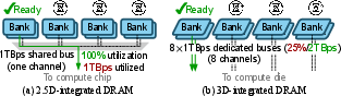
- 2.5D packaging technology: A chip integration approach placing multiple dies side-by-side on an interposer, limiting inter-die bandwidth by perimeter. "2.5D packaging technology (e.g., H100~\cite{h100} and TPU~\cite{tpu_v4i})"
- 2D mesh: A network-on-chip topology where nodes are arranged in a 2D grid with nearest-neighbor links. "2D mesh"
- 3D integration: Vertical stacking of silicon dies connected by TSVs to boost inter-die bandwidth and density. "3D integration also enables superior bandwidth scalability."
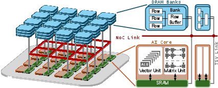
- 3D-stacked AI chip: An AI chip architecture stacking DRAM above compute cores to provide high-bandwidth memory access. "The 3D-stacked AI chip enables ultra-high memory bandwidth between compute and memory by stacking numerous DRAM banks atop many AI cores in a distributed manner."
- all-to-all: A NoC topology where every node can directly connect to every other node. "Among the popular NoC topologies (mesh, torus, and all-to-all)"
- allReduce(): A collective communication operation that aggregates data (e.g., sums) across cores and distributes the result to all of them. "For example, \mbox{\textstt{allReduce()} comprises multiple \mbox{\mvdata{} functions for moving partial results among cores and multiple \mbox{\comp{} functions for reducing partial results locally on each core;"
- bank interleaving: A memory scheduling technique that distributes successive accesses across banks to improve throughput. "maximize bank interleaving"
- bandwidth density: Memory bandwidth per unit chip area, indicating how much bandwidth can be delivered within a given die footprint. "3D integration technology can achieve a bandwidth density of 400 GB/s per 0.02 mm of die area with current fabrication technology"
- bandwidth utilization: The extent to which available memory or link bandwidth is actually used by the system. "which makes bandwidth utilization a new challenge."
- BF16: Brain floating-point 16-bit format, a reduced-precision floating-point type used to accelerate AI workloads. "parameters at BF16 precision"
- burst granularity: The hardware-defined unit size at which DRAM transfers data to/from memory. "at burst granularity."
- compute paradigm: The strategy for organizing computation and communication across cores (e.g., SPMD, dataflow, compute-shift). "Compute paradigms are critical to 3D AI chip performance,"
- compute-shift: A compute paradigm that shifts computation to overlap with data movement for higher utilization. "Among existing compute paradigms, compute-shift performs the best"
- core group: A set of adjacent cores that coordinate DRAM access patterns to reduce conflicts and improve utilization. "we group physically adjacent cores into core groups and synchronize their DRAM accesses within each group via a hardware tracker."
- dataflow: A compute paradigm where computation is structured around the flow of data through operations and hardware units. "applied computing paradigms (e.g., single-program-multiple-data (SPMD)~\cite{alpa,xla}, dataflow~\cite{samba-whitepaper,inter-layer}, compute-shift~\cite{t10,waferllm:osdi2025})"
- dimension-ordered mapping: Mapping tiles to cores in a fixed dimension order to minimize communication distance and hops. "a dimension-ordered mapping can minimize the NoC overhead"
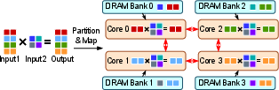
- distributed memory architecture: A memory organization where memory modules are physically distributed across the chip, leading to non-uniform access latency. "With this distributed memory architecture, each AI core is connected to the DRAM {banks} directly on top of it via TSVs."
- DRAM bank: An independently accessible subarray within a DRAM device that services requests via a row buffer. "A grid of DRAM banks is stacked on top of the cores and NoC, and there are multiple layers of DRAM banks to scale capacity."
- DRAM burst: A contiguous block of data transferred in a single DRAM operation. "Each request accesses one DRAM burst."
- DRAM channel: A set of DRAM banks and associated bus/interface that operate together to serve memory requests. "On a 3D AI chip, a DRAM channel contains one or more banks that share one TSV bus."
- DRAM refreshes: Periodic operations to restore charge in DRAM cells, temporarily blocking accesses to refreshed rows. "cannot capture the impact of DRAM refreshes."
- energy efficiency: Performance delivered per unit of energy, often improved by reducing execution time for memory-bound workloads. "the energy efficiency of a 3D AI chip will be improved."
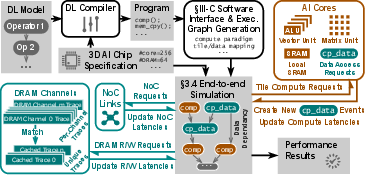
- event-driven simulation: A simulation approach that advances system state by processing discrete events in time order. "through an event-driven simulation of all hardware components"
- execution graph: A directed graph of computation, communication, and synchronization events capturing dependencies and scheduling. "VoxelSim constructs execution graphs to track the end-to-end execution progress"
- FLOPS utilization: The fraction of a processor’s peak floating-point operations per second that is achieved in practice. "AI cores have reached high FLOPS utilization"
- fused operator: A compiler- or runtime-merged operation combining multiple primitives to reduce memory traffic and overhead. "when a fused operator concurrently accesses 3 or more inputs"
- MatMul: Matrix multiplication, a core linear algebra operation in AI workloads. "a matrix unit (e.g., systolic array) handles large matrix multiplication (MatMul) operations at high throughput."
- monolithic, uniform memory architecture: A memory model where all cores see a single memory with near-uniform latency and bandwidth. "assume a monolithic, uniform memory architecture"
- network-on-chip (NoC): The on-die interconnection network linking cores and other components for data movement. "interconnected via a network-on-chip (NoC) layer"
- NoC contention: Performance degradation due to multiple transfers competing for the same NoC links and resources. "NoC contention and data transfer overhead."
- NoC hops: The number of link traversals a packet takes across the NoC from source to destination. "reduce the number of NoC hops per data transfer."
- NoC link bandwidth: The data rate of individual NoC links, determining throughput for inter-core transfers. "NoC topologies and link bandwidth"
- NoC topology: The structural arrangement of nodes and links in the on-chip network (e.g., mesh, torus, all-to-all). "Among the popular NoC topologies (mesh, torus, and all-to-all)"
- per-core SRAM: Fast on-core scratchpad memory used to buffer data and reduce DRAM accesses. "per-core SRAM capacity"
- prefetch: Proactively copying data to a closer memory (e.g., SRAM) before it is needed to hide latency. "a runtime copy (prefetch) of a tensor part."
- prefill: The initial phase of LLM inference that processes the prompt/context before token-by-token decoding. "compute/NoC-bound workloads like LLM prefill"
- processing-in-memory (PIM): Architectures performing computation near or within memory to reduce data movement overheads. "Some processing-in-memory (PIM) implementations share architectural features with 3D AI chips"
- power density: Power consumed per unit area, a key thermal constraint in stacked designs. "power density (i.e., power per area)"
- row buffer: A DRAM structure holding the currently active row to service column accesses efficiently. "whose contents are accessed via the row buffer."
- row-buffer conflicts: Performance penalties when DRAM must close one open row and open another due to alternating accesses. "minimizing the row-buffer conflicts"
- single-program-multiple-data (SPMD): A parallel programming model where multiple processing elements run the same program on different data partitions. "single-program-multiple-data (SPMD)"
- SRAM: On-chip static memory used for fast, low-latency data storage compared to DRAM. "a fast local SRAM buffers the data from DRAM"
- systolic array: A regular array of processing elements optimized for high-throughput matrix operations. "a matrix unit (e.g., systolic array)"
- tensor parallelism: A parallelization strategy that partitions tensor dimensions across devices/cores to distribute computation. "with tensor parallelism"
- tensor-to-bank mapping: The scheme for assigning tensor shards to specific DRAM banks to balance bandwidth and reduce conflicts. "software-aware {tensor-to-bank} mapping scheme"
- Through-Silicon Vias (TSVs): Vertical electrical interconnects passing through silicon to connect stacked dies. "Through-Silicon Vias (TSVs) act as vertical electrical interconnects that pass through the silicon substrate itself."
- tile-to-core mapping: The policy for assigning partitioned computation tiles to specific cores to minimize communication. "tile-to-core mapping"
- torus: A NoC topology where edges wrap around, reducing average path lengths compared to meshes. "Among the popular NoC topologies (mesh, torus, and all-to-all)"
- TSV bus: A vertical data bus composed of TSVs connecting cores to stacked DRAM banks. "one or more banks that share one TSV bus."
Collections
Sign up for free to add this paper to one or more collections.