- The paper demonstrates that integrated photonics, via a comprehensive EPDA approach, enables ultra-low latency and high bandwidth for AI workloads.
- It introduces the SimPhony framework to benchmark end-to-end energy efficiency and compute density, comparing photonic accelerators to state-of-the-art GPUs.
- It applies AI-assisted inverse design and layout automation to produce compact, scalable photonic circuits that adapt to dynamic machine intelligence requirements.
Harnessing Photonics for Machine Intelligence: A Systems Perspective
Introduction
The exponential escalation in machine intelligence workloads—especially with the evolution from basic deep neural networks to foundation models—has fundamentally altered the computational landscape. Classical scaling via Moore's Law and Dennard scaling has stalled, precipitating the need to explore alternative compute substrates that can circumvent the energy, bandwidth, and memory bottlenecks inherent to advanced silicon CMOS. Integrated photonics has emerged as a prominent candidate, leveraging the intrinsic physical advantages of light—ultra-low latency, extensive bandwidth density, and superior energy efficiency—to address modern AI’s growing requirements. This paper systematically reframes photonic computing through cross-layer systems analysis and proposes a holistic electronic-photonic design automation (EPDA) approach, providing critical insights for architecting scalable, efficient, and robust photonic AI systems (2604.10841).
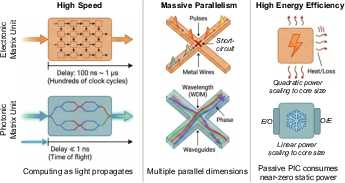
Physical Advantages of Photonic Computing
Photonic computing derives its strengths from fundamental physical phenomena, enabling computing regimes not attainable through electronics. Three principal advantages are delineated:
Benchmarking Photonic AI: System-Level Evaluation and Bottleneck Analysis
While device-level gains are substantial, system-level deployability is determined by the interaction between the photonic core and electronic-mixed-signal periphery. The paper implements a cross-layer simulation framework, SimPhony, to conduct fair benchmarking of end-to-end energy efficiency (TOPS/W) and compute density (TOPS/mm2) for various photonic accelerator designs relative to SOTA electronic GPUs.
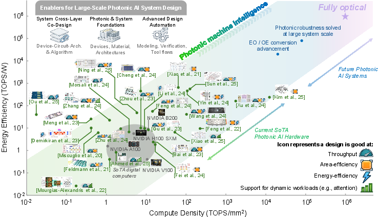
Figure 2: System-level energy efficiency vs. compute density comparison between silicon-photonic accelerators and digital GPUs.
SimPhony provides architecture-centric modeling that incorporates not only photonic computation, but also DAC/ADC conversion, laser power under practical optical link budgets, and the impact of workload/architecture mapping. These results evidence significant heterogeneity across photonic designs—while architectures optimized for dynamic workloads and minimized E/O overheads (e.g., time-multiplexed crossbars) can surpass GPUs on both density and energy metrics, core-centric approaches (e.g., MZI meshes, static MRR banks) frequently underperform once realistic system taxes are included.
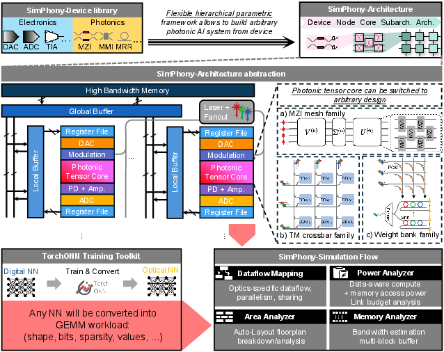
Figure 3: SimPhony framework for parametric, device-to-architecture photonic system modeling, energy/area analysis, and real-world workload binding.
Impact of Workload Dynamics and Parameter Scaling
The transition from statically programmed DNNs (CNNs, MLPs) to dynamic, attention-rich Transformers redefines bottlenecks in photonic hardware. The authors show that MZI mesh-based architectures—optimized for static linear projections—face prohibitive reconfiguration costs and cannot efficiently accelerate dynamic GEMM workloads (e.g., attention).
In contrast, designs such as time-multiplexed crossbars maintain high spectral and temporal operand reusability, enabling practical acceleration of dynamic workloads at energy efficiencies exceeding SOTA GPUs.
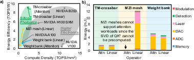
Figure 4: (a) Energy efficiency and compute density comparison, (b) componentwise energy breakdown across three photonic tensor families—highlighting the increasing dominance of E/O conversion and peripheral costs.
Ambient system efficiency remains most sensitive to bit precision (conversion power scales exponentially) and memory-conversion bandwidth, setting a practical “precision wall” and underscoring the centrality of E/O interface minimization in scalable analog photonic computing.
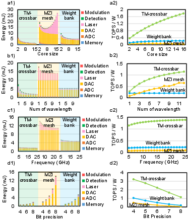
Figure 5: Parameter scaling analysis: core size, wavelength parallelism, bit precision, and clock frequency—exposing the nonlinear penalty of bit-precision scaling and the beneficial amortization from parallelism.
Achieving large-scale, reproducible photonic AI systems necessitates a shift from bespoke, component-level demonstrations to an integrated, automation-driven design flow.
- AI-Assisted Device and Circuit Simulation: The paper reviews deep learning- and operator-based surrogates for Maxwell’s equations, accelerating EM simulation for high-dimensional device/circuit synthesis and enabling differentiable, system-aware optimization.
- Photonic Component Inverse Design: The authors highlight the transition from manual topology tuning to large-DoF, goal-oriented inverse design workflows—combining adjoint-gradient optimization, evolutionary heuristics, and AI-based generative approaches—to synthesize ultra-compact, fabrication-constrained photonic components and circuit blocks, with orders-of-magnitude area reduction.
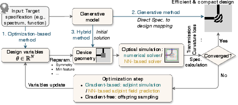
Figure 6: Photonic component inverse design flows: optimization-based, generative, and hybrid approaches.
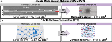
Figure 7: Inverse-designed photonic circuit blocks achieve massive footprint reduction versus manual layouts, enabling denser functional integration.
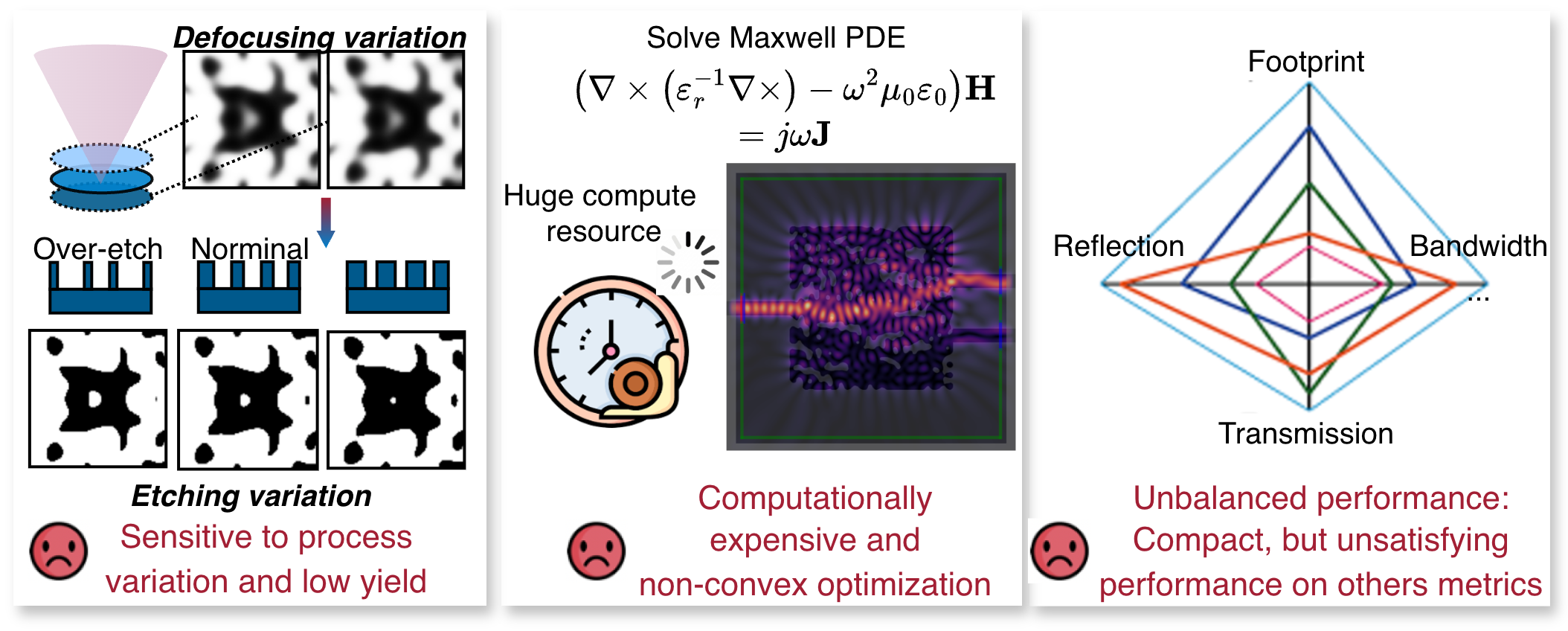
Figure 8: Key challenges in photonic inverse design: process-aware manufacturability, simulation cost, local minima, and multiphysics balancing.
- EPDA for Layout Automation: Modern photonic integrated circuits (PIC) demand DRC-aware, placement- and routing-informed layout synthesis, with a focus on system-level yield, crosstalk control, waveguide/metal detour co-optimization, and integration with advanced packaging. The survey tracks the rapid progression from schematic-driven manual flows through agentic, language-guided, and multi-layer 3D integration-focused physical design tools.
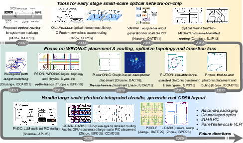
Figure 9: Evolution of PIC physical design automation: manual, topology-aware, and next-generation agentic/generative flows.
Implications and Future Directions
This review asserts that future photonic AI accelerators must prioritize workload-adaptive programmability, robust accuracy under evolving application dynamics, and system-centric optimization that explicitly targets energy/density Pareto frontiers. The field's progress will be determined by the convergence of standardized, workload-driven benchmarking, generalized, robust EPDA toolchains, and cross-layer co-design methodologies that can encode photonic, electronic, and algorithmic requirements in a unified framework (2604.10841).
Key prospective trends include:
- Systematic benchmarking with realistic interface/modeling constraints
- Compiler-grade workload-to-system mapping for heterogeneous PIC + electronic SoC architectures
- Closed-loop, yield- and process-aware device-circuit-system co-optimization
- Agentic, ML-driven design tools integrating inverse design, layout generation, and physical verification
Conclusion
The trajectory for photonic machine intelligence is shifting from isolated feasibility to sustainable, system-level scalability. The paper demonstrates that genuine, reproducible photonic advantage is only achievable via holistic cross-layer optimization and automation, not via device-centric improvement alone. The deployment of robust, flexible, and high-fidelity photonic accelerators will necessitate the maturation of full-stack EPDA, encompassing device, circuit, architecture, and physical design layers. This EPDA-driven approach is essential for photonics to co-evolve with, and enable, the ever-expanding computational demands of modern AI.