Sub-kelvin thermal conductivity of substrates and on-chip routing in quantum integrated systems
Abstract: The development of large-scale quantum systems increasingly relies on the close integration of heterogeneous components such as qubits, control electronics, and readout circuits, making thermal management at cryogenic temperatures a central challenge in such architectures. In this work, we present an experimental thermal study of two building blocks of such systems: the substrate and the on-chip routing. We first investigate the sub-kelvin thermal conductivity of four substrate materials: high-resistivity silicon, low-resistivity silicon, borosilicate, and sapphire. We report that high-resistivity silicon exhibits the highest thermal conductivity among the substrates studied ($5\cdot10{-2}$~W/m$\cdot$K at 300~mK), while low-resistivity silicon, borosilicate, and sapphire show lower values ($8\cdot10{-4}$~W/m$\cdot$K, 2$\cdot10{-3}$~W/m$\cdot$K, and 2$\cdot10{-3}$~W/m$\cdot$K at 300~mK, respectively). Ballistic conductance evaluation using a finite-element non-equilibrium Green's function approach further allows us to extract the phonon mean free path in each substrate and gives insights into the involved scattering mechanisms. Additionally, we employ a dedicated test vehicle to evaluate the impact of on-chip routing on the thermal conductance of the system. Our measurements with superconducting Nb routing lines reveal that the routing increases the in-plane thermal conductance of the system, but the substrate remains the dominant heat path. These results highlight the critical role of the substrate choice within quantum systems and underscore the importance of function partitioning through 3D integration approaches for more efficient thermal management in quantum architectures.
Paper Prompts
Sign up for free to create and run prompts on this paper using GPT-5.
Top Community Prompts
Explain it Like I'm 14
What is this paper about?
This paper looks at how heat moves through the “base layers” of tiny, super-cold quantum computer chips. These chips must work below 1 kelvin (that’s colder than outer space). The authors measure how well different materials carry heat at those temperatures and test how adding on‑chip wiring (the metal lines that connect parts of a chip) changes the way heat spreads. The goal is to help design quantum systems that don’t overheat their delicate qubits.
What questions did the researchers ask?
They focused on two simple questions:
- Which common chip materials carry heat best below 1 kelvin?
- Does adding typical on‑chip wiring (especially superconducting niobium lines) make heat spread more, or does the substrate (the main chip “base”) still dominate?
How did they study it?
Measuring heat flow with a heater and a thermometer
- Think of heat like traffic. If a road is wide and smooth, cars (heat) move easily. If it’s narrow or bumpy, traffic slows down. Here, the “road” is the material inside the chip.
- The team glued a long, thin piece of each material to a cold copper plate inside a cryostat (a super-cold fridge). They attached:
- A tiny heater on one end (to add a known amount of heat).
- A tiny thermometer near the heater (to see how hot that end gets).
- By turning the heater up step by step and measuring how much the temperature rose, they worked out the material’s thermal conductivity: a number that tells you how easily heat moves through it.
They tested four substrates:
- High‑resistivity (very pure) silicon
- Low‑resistivity (doped) silicon
- Borosilicate glass
- Sapphire
Understanding what limits heat flow: “phonons” and “mean free path”
- Below 1 kelvin, heat in solids mostly moves as tiny vibrations of the atoms called phonons (you can imagine them as ripples or “heat waves” in the crystal).
- Mean free path (MFP) is how far a phonon goes before it bumps into something (like an impurity, a defect, or a surface) and changes direction—just like how far a car goes before hitting a red light.
- To estimate MFP, they compared:
- The “best possible” heat flow if phonons never bumped into anything (a computer model called ballistic conductance).
- The actual measured heat flow.
- From that comparison, they calculated the MFP and learned what was causing most of the “red lights” for heat.
Note: They used an advanced, but for our purposes simple-to-grasp, computer method to get the best‑case heat flow (a finite‑element non‑equilibrium Green’s function model). You can think of it as: “simulate the smoothest road possible,” then see how the real road differs.
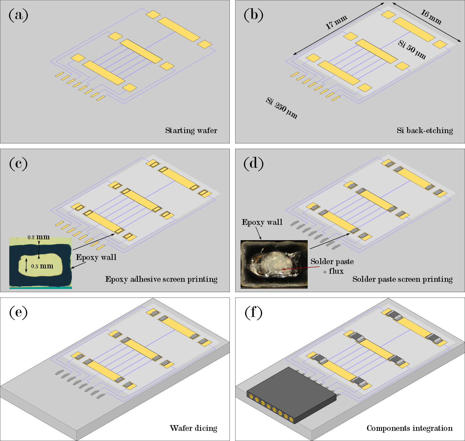
Testing on‑chip wiring
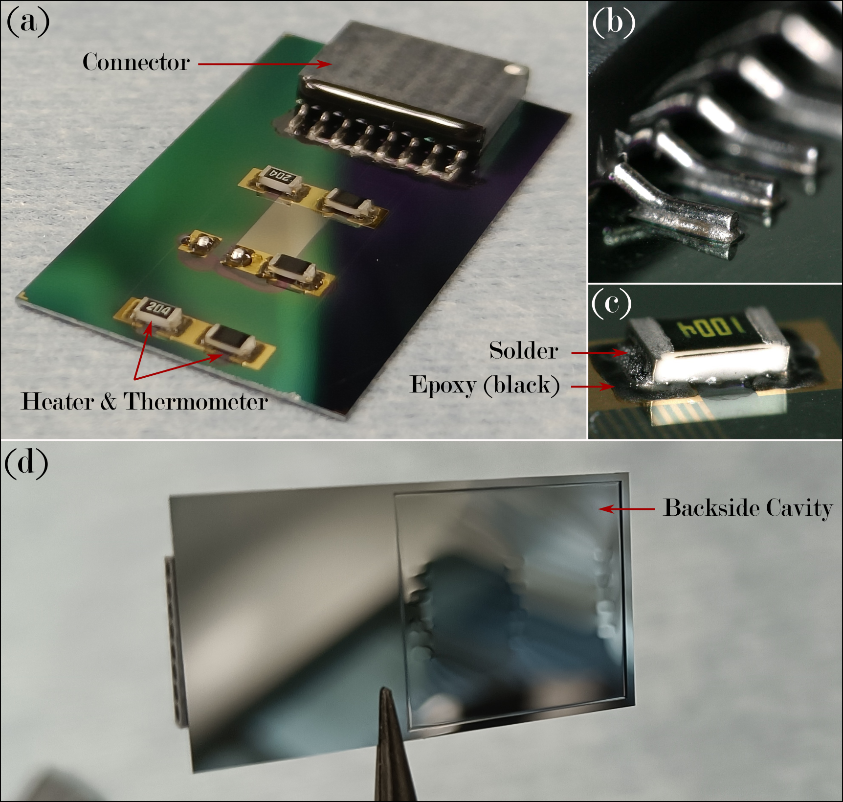
- They also built a small test chip on low‑resistivity silicon with:
- Superconducting niobium (Nb) routing lines (superconductors carry electricity with no resistance and, at these temperatures, their electrons don’t carry heat like normal metals do).
- Gold pads (for good thermal and electrical contact).
- They thinned the silicon under the wiring (made a backside cavity) to reduce the substrate’s heat path, then measured how heat moved from one pad to another with two thermometers and one heater.
What did they find?
Here are the key results in simple terms:
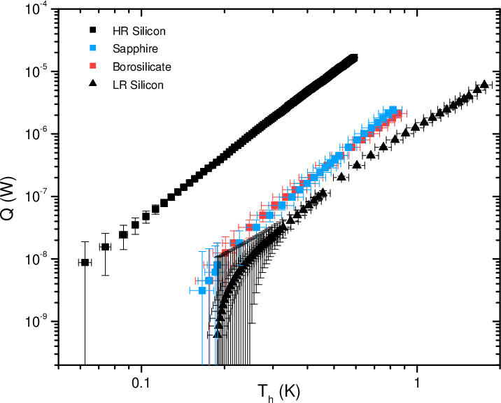
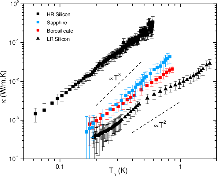
- High‑resistivity (HR) silicon (very pure)
- Best heat carrier at 0.3 K: about 5×10⁻² W/m·K.
- MFP is very long (around a few millimeters), meaning phonons mainly bounce off the sample’s edges, not impurities. The sample’s size, not dirtiness, limits heat flow.
- Low‑resistivity (LR) silicon (boron‑doped, with more oxygen from the growth method)
- Much worse at carrying heat: about 8×10⁻⁴ W/m·K at 0.3 K (roughly 60× lower than HR silicon).
- MFP is short (tens of micrometers) and shrinks as temperature rises. That’s because phonons bump into dopant atoms and defects—like many extra traffic lights on the road.
- Sapphire
- Heat flow: about 2×10⁻³ W/m·K at 0.3 K.
- The temperature trend looks like a clean crystal (it rises like T3), but the actual heat flow is much lower than in big, perfect sapphire. The MFP is short (~50 µm), likely because of structural disorder (tiny crystal grains act like many small speed bumps).
- Borosilicate glass (amorphous, not a crystal)
- Similar heat flow to sapphire at 0.3 K: about 2×10⁻³ W/m·K.
- The temperature trend is different (rises like T2), which is typical of glasses. Heat‑carrying phonons don’t travel ballistically; their MFP is short and strongly temperature‑dependent.
- On‑chip routing (Nb lines + Au pads) on LR silicon
- Adding routing increased the in‑plane thermal conductance (the “ease” of heat flow sideways) by about 4× at 0.5 K compared to bare low‑resistivity silicon with the same geometry.
- Still, the substrate (silicon) remained the main highway for heat. The routing adds lanes, but the base road (the substrate) is the biggest factor.
A practical warning from the measurements:
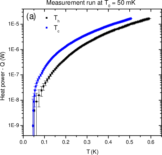
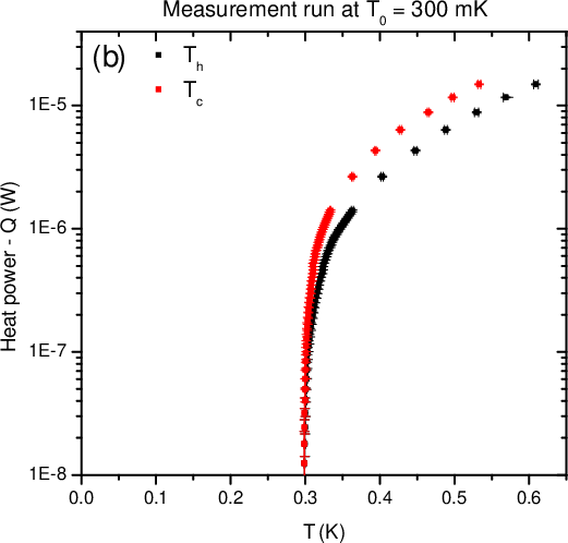
- Even tiny powers (as low as 1–10 nanowatts) raised temperatures and created measurable gradients on centimeter‑scale samples at ~300 mK. That’s extremely small—far below the microwatts that today’s cryogenic control electronics often use per qubit.
- This shows how easy it is to overheat nearby qubits if heat is not carefully managed.
Why is this important?
Quantum chips need many qubits and nearby control electronics. But qubits are extremely sensitive to heat—warming them even a little can make them lose their quantum state (decohere). This study shows:
- Which substrates help carry heat away quickly (HR silicon) and which help keep heat from spreading (LR silicon, glass).
- How much wiring changes the picture (some increase in heat flow, but the substrate still dominates).
- How shockingly small power can disturb temperatures at these ultra‑cold levels.
In short, thermal design is not a detail—it’s a central challenge for building large, reliable quantum systems.
What does this mean for the future?
- Pick your substrate on purpose:
- Use HR silicon when you want to remove heat efficiently (cool hot electronics faster).
- Use LR silicon or glass when you want to thermally isolate sensitive areas (protect qubits), but beware: isolation also traps heat if you need to get rid of it.
- Don’t rely on on‑chip wiring to carry away much heat; the substrate rules the game in planar chips.
- Keep hot control electronics thermally separated from qubits:
- Use 3D integration or system‑in‑package designs to stack and separate functions.
- Consider placing the power‑hungry electronics at a warmer stage (like 4 K) and connect with thermally resistive links.
- Big picture: To scale up quantum computers, we must treat heat like a first‑class design problem—exactly which materials, layouts, and stackups we choose will decide whether qubits stay cold and coherent.
Knowledge Gaps
Knowledge gaps, limitations, and open questions
The following points identify what is missing, uncertain, or left unexplored in the study, and suggest concrete follow-ups for future work.
Experimental methodology and comparability
- Parasitic heating (Q0) limits low-temperature access and accuracy: quantify and eliminate Q0 (e.g., fully isolated heater drive, differential wiring, independent ground, in situ four-wire calorimetry) to enable measurements down to base temperature and reduce systematic bias in G and κ.
- Copper–substrate boundary resistance was validated only for silicon and assumed similar for other materials; directly measure Rb for each substrate (sapphire, borosilicate) using dual-thermometer or time-domain methods to ensure the interface is not the bottleneck.
- Sample geometries differ (sapphire thinner/smaller than others), confounding material comparisons; repeat measurements with matched L, w, d across all materials to isolate intrinsic behavior from Casimir-size effects.
- Single specimens per material and vendor-specific wafers were used; assess wafer-to-wafer and vendor variability (multiple samples, multiple lots) to quantify spread due to impurities, polishing, and processing.
- Neglected parallel heat paths (NbTi wiring, adhesives, passivation) were justified qualitatively; establish quantitative upper bounds (with and without connections; replace adhesives; measure oxide-only controls) to bound their contributions to G.
- RuO2 thermometer self-heating and calibration on heterogeneous substrates were not systematically validated; provide cross-calibration (e.g., fixed points, noise thermometry) and quantify self-heating errors vs. applied heater power.
Substrate physics and mechanisms
- HR silicon deviates from ideal T3 scaling (observed ~T2.4); disentangle contributions from partial specular boundary scattering, residual isotope/defect scattering, and surface roughness by:
- Varying thickness/width to test Casimir scaling and specularity (Ziman parameter) dependence.
- Comparing surfaces with controlled roughness/etching and different oxide terminations.
- Testing isotopically enriched vs. natural Si.
- LR silicon doping details (carrier density, oxygen, carbon) are not directly measured for the specific sample; determine actual impurity/defect concentrations (SIMS, FTIR for oxygen, Hall for carriers) and systematically sweep doping and oxygen levels to map κ(T) and λ(T).
- The phonon–hole scattering model uses a single effective λ with simplified parameters; perform spectral MFP reconstruction (e.g., using frequency-dependent BTE or MFP spectroscopy) to capture mode- and frequency-dependent scattering in LR Si.
- Sapphire’s κ is ∼100× lower than bulk with T3 but temperature-independent λ ≪ Casimir; verify the hypothesized structural disorder by microstructural characterization (XRD/EBSD/TEM, AFM for roughness), and correlate grain size/orientation with κ(T) and λ(T).
- Sapphire anisotropy and orientation effects are not explored; measure κ along multiple axes and wafer orientations (C-, A-, M-plane), and assess polishing-induced damage layers vs. bulk.
- Borosilicate is modeled with SiO2 elastic constants in ballistic conductance; obtain low-temperature elastic constants for the specific borosilicate composition and repeat G0 calculations to reduce modeling error.
- Amorphous transport in borosilicate is interpreted via TLS phenomenology without parameter extraction; extract TLS parameters (e.g., from C(T), internal friction) and test consistency with κ(T), including thickness dependence to rule out residual boundary effects.
Modeling assumptions and MFP extraction
- The G = G0 λ/(L+λ) interpolation assumes a single, energy-independent λ; extend to mode- and frequency-resolved transport (BTE/FENEGF hybrid or Landauer with spectral mean free paths) to improve λ(T) inference and avoid fitting degeneracies.
- Ballistic conductance G0 relies on continuum elastic constants and assumes perfect contacts; evaluate sensitivity to uncertainties in elastic constants at sub-kelvin temperatures and to phonon focusing/anisotropy, and validate G0 against reference samples with known Casimir limits.
- Boundary scattering specularity and surface state (oxide, glue contact, polishing damage) are not incorporated in λ analysis; explicitly model/specify specularity parameters and verify via controlled surface treatments.
On-chip routing study
- Routing contribution is inferred indirectly (routing + pads + passivation treated as a lumped parallel path); deconvolve contributions by:
- Varying Nb line width/length/density and Au pad size independently.
- Testing “pads-only,” “routing-only,” and “oxide-only” controls with identical cavities.
- Replacing Nb with a normal metal (Cu/Al) and with different superconductors (Al, NbTiN) to quantify electronic vs. phononic channels.
- Electron–phonon decoupling in Au pads is neglected above ~100 mK; verify onset experimentally (vary pad volume, use different metals) and include e–ph limits in the thermal model for ≤300 mK operation.
- Encapsulation/passivation (∼500 nm SiO2) is omitted in modeling; quantify its in-plane and interfacial thermal roles (thickness sweeps, different dielectrics, patterned vs. continuous films).
- Backside cavity geometry and residual Si thickness are assumed ideal; map conductance vs. cavity depth, lateral clearance, and framing thickness to optimize thermal isolation and to validate the 1D assumption with full 3D simulations.
- Only two base temperatures (50 mK with parasitic heating and 300 mK) were explored; perform continuous base-T sweeps to separate intrinsic T-dependences of routing vs. substrate and to identify any low-T crossovers (e.g., e–ph limits, quasiparticles).
System-level relevance and external validity
- Suspended or partially freed dies do not represent standard packaging with full-area die attach; quantify vertical heat extraction (Kapitza and adhesive boundary resistances) in realistic mounts and re-evaluate allowable dissipation thresholds under practical chip–holder interfaces.
- Only in-plane conduction is characterized; integrate through-thickness pathways and chip–package interfaces in a full thermal network (including TIMs, interposers, bumps/TSVs) to predict thermal crosstalk in SoC vs. SIP stacks.
- The “tens of nW at 300 mK” dissipation tolerance is an order-of-magnitude estimate from simplified conditions; establish design rules via calibrated multi-physics models validated against devices with realistic heat sources (active cryo-CMOS macros) and measured chip temperature maps (e.g., Johnson noise thermometry, on-chip thermometers).
- The recommendation toward SIP/3D integration is qualitative; quantify the thermal resistance of candidate interconnects (indium bumps, superconducting flex, micro-cables) at sub-kelvin and benchmark achievable thermal isolation vs. system-level bandwidth/latency constraints.
- RF performance vs. thermal management trade-offs are noted but not quantified; co-optimize substrate choice for both (e.g., HR-Si vs. sapphire) by measuring RF loss tangent vs. κ(T) on identically processed wafers.
Measurement uncertainty and reporting
- Uncertainty quantification is relegated to supplemental material and not propagated to κ(T), G(T), and λ(T) curves; provide full error bars (including geometry, thermometer calibration, Q0, differentiation noise, and model uncertainty in G0) and perform sensitivity analysis.
- Reproducibility across cooldowns and mounting cycles is not reported; repeat measurements after re-mounting and re-gluing to bound variability from interfaces and assembly.
These gaps, if addressed, would enable more accurate material comparisons, clarify scattering mechanisms, isolate routing contributions, and produce system-level design rules for thermal management in quantum integrated systems.
Practical Applications
Overview
Based on the paper’s measurements of sub‑kelvin thermal conductivity and mean free path (MFP) across common substrates (high‑resistivity Si, low‑resistivity Si, borosilicate glass, sapphire), plus the test-vehicle study of superconducting Nb on‑chip routing, the following applications translate the findings into concrete decisions, tools, and workflows for industry, academia, policy, and (indirectly) daily life. Each item notes sectors, what can be built or done, and key assumptions/dependencies that affect feasibility.
Immediate Applications
- Substrate selection guidelines for cryogenic ICs (sectors: semiconductors, quantum computing hardware, packaging)
- Action: Use high‑resistivity (HR) float‑zone Si for heat spreading (κ ≈ 5×10⁻² W/m·K at 300 mK) and low‑resistivity (LR) Czochralski Si for thermal isolation (κ ≈ 8×10⁻⁴ W/m·K at 300 mK). Treat borosilicate and sapphire as low‑κ options (~2×10⁻³ W/m·K at 300 mK) with different T‑scalings (T² vs T³).
- Tools/workflows: Update PDK/DFM notes and substrate BOMs for cryo stacks; incorporate κ(T) and exponents (HR‑Si ~T².⁴, LR‑Si ~T².², sapphire ~T³, borosilicate ~T²) into pre‑layout thermal rules of thumb and spreadsheets.
- Assumptions/dependencies: Geometry strongly affects effective κ at mK (boundary scattering); wafer purity (oxygen/boron) and surface condition matter; cryostat interface quality dominates vertical heat extraction.
- Power‑budget and floorplanning rules for co‑integrated cryo‑CMOS and qubits (sectors: quantum computing hardware, EDA/software)
- Action: Adopt conservative placement rules that limit local dissipation near qubits to O(10 nW) at 300 mK in centimeter‑scale dies; reserve µW‑class loads for thermally isolated dies or higher stages (e.g., 4 K).
- Tools/workflows: Add “nW-level proximity caps” and keep‑out zones around qubits in floorplanning; checklist gates for thermal approval.
- Assumptions/dependencies: Study used suspended samples; full‑die gluing can raise the threshold; chip‑to‑cold‑plate boundary resistance (Kapitza) and packaging dominate vertical heat removal.
- EDA library updates with sub‑kelvin material models (sectors: EDA/software, semiconductors)
- Action: Integrate κ(T) fits and MFP‑limited scaling for HR‑Si, LR‑Si, sapphire, borosilicate into thermal co‑simulation engines and system models.
- Tools/workflows: Parameterized compact models for κ(T); templates for die‑scale 1D/2D thermal networks; import into Ansys, COMSOL, Cadence thermal plugins.
- Assumptions/dependencies: Values are geometry‑dependent in boundary regime; amorphous modeling via continuum elasticity is approximate.
- Wafer procurement and QA specifications (sectors: materials, foundries, supply chain)
- Action: Specify float‑zone HR‑Si with low oxygen (<~10¹⁵ cm⁻³) for maximal κ; for isolation, accept CZ LR‑Si with defined boron/oxygen ranges; for sapphire, require crystallite/grain size control; document surface roughness/polish.
- Tools/workflows: Incoming inspection with XRD for sapphire crystalline size, FTIR for oxygen in Si, resistivity mapping; vendor scorecards tied to κ(T) risk.
- Assumptions/dependencies: Cost/availability of float‑zone wafers; differences across orientations; supplier process variability.
- Routing and back‑side thinning choices (sectors: semiconductors, packaging, process integration)
- Action: Prefer superconducting (e.g., Nb) routing over normal metals to suppress electronic heat conduction; expect substrate to dominate in‑plane heat path; use local back‑side cavities/thinning to reduce substrate G where needed.
- Tools/workflows: Design rules for routing density/width vs thermal impact; process modules for localized back‑side thinning under hot blocks; test vehicles mirroring the paper’s layout for quick characterization.
- Assumptions/dependencies: Mechanical integrity/yield of thinned regions; added process complexity; parasitic heat via pads and passivation.
- Cryogenic packaging guidelines at mK (sectors: packaging, cryogenics)
- Action: Maximize die‑to‑cold‑plate contact area and control glue interfaces; use high‑conductance mounts when cooling is desired, and tuned/limited contact when isolation is desired; explicitly budget chip‑cryostat boundary resistance.
- Tools/workflows: Standardized silver‑epoxy area targets, surface finishes, torque specs; verification via dual‑thermometer control tests.
- Assumptions/dependencies: Kapitza resistance varies with materials/roughness/pressure; reliability over thermal cycles.
- Rapid sub‑kelvin thermal characterization workflow (sectors: metrology, R&D labs)
- Action: Deploy the SMD RuO₂ thermometer + heater method with long superconducting leads and AC bridge readout; apply dQ/dT differentiation to extract κ(T); include a cold‑side control thermometer to verify non‑bottlenecked interfaces.
- Tools/workflows: Bill of materials, wiring guides, data‑processing scripts; routine QA across wafer lots or after processes (e.g., CMP, etch).
- Assumptions/dependencies: Need to mitigate parasitic Q₀ and thermometer self‑heating; careful calibration and shielding.
- FE‑NEGF ballistic conductance + MFP extraction for materials screening (sectors: academia, advanced R&D, EDA)
- Action: Use finite‑element non‑equilibrium Green’s function simulations of ballistic conductance per area to back‑out MFP from measurements, attributing dominant scattering (boundary, doping, grain boundaries).
- Tools/workflows: FE‑NEGF packages and material elastic constants databanks; automated MFP extraction scripts for wafer/process comparisons.
- Assumptions/dependencies: Validity is strongest for crystalline materials; amorphous solids need care; expertise and compute resources required.
- Thermal design for cryogenic photonics and sensors (sectors: photonics, superconducting detectors, astronomy)
- Action: Leverage low κ and T² scaling of borosilicate for thermal isolation around MKIDs/TESs or integrated photonics at mK; plan cooling paths deliberately.
- Tools/workflows: Device‑level thermal RC networks incorporating borosilicate κ(T); layout keep‑ins/outs for isolation trenches.
- Assumptions/dependencies: Mechanical and optical requirements; process compatibility.
- System architecture choices for cryo stacks (sectors: systems engineering, data centers, quantum services)
- Action: Place dissipative cryo‑CMOS at 4 K when feasible and connect with thermally resistive superconducting flex; reserve mK stages for qubits and ultra‑low‑power readout.
- Tools/workflows: Reference architectures with cooling‑power budgets at each stage; cable/lineup libraries with measured thermal conductance.
- Assumptions/dependencies: Signal latency, wiring complexity, and system‑level calibration trade‑offs.
Long‑Term Applications
- Thermally decoupled 3D SIP architectures (sectors: advanced packaging, quantum hardware)
- Vision: Widespread use of 3D system‑in‑package with thermally resistive interconnects (e.g., engineered indium bumps, phononic barriers, superconducting flex) to partition hot control chips from mK‑stage qubits.
- Potential products: High‑Rth interposers; phononic Bragg reflectors in interconnect stacks; “thermal vias” with engineered resistance.
- Dependencies: Manufacturability, interconnect reliability, RF integrity, and parasitic inductance/capacitance control.
- Standardized sub‑kelvin materials database and cryo‑PDK (sectors: EDA, standard bodies, foundries)
- Vision: Community‑curated κ(T) and MFP datasets for common substrates, films, and stacks, validated across foundries and integrated into commercial EDA.
- Potential products: IEEE/NIST‑aligned models; multi‑vendor compatible cryo thermal libraries.
- Dependencies: Measurement standardization, IP/data sharing incentives, and cross‑tool interoperability.
- Engineered crystalline quality for sapphire and Si (sectors: materials, wafer suppliers)
- Vision: Grain‑size/specification control in sapphire to recover desired T³ κ; oxygen/boron control in Si to tune MFP and κ on demand.
- Potential products: “Thermal‑grade” sapphire and Si wafers with guaranteed sub‑kelvin thermal specs.
- Dependencies: Growth process advances, metrology, and cost/volume viability.
- Tunable thermal substrates and barriers via doping and defects (sectors: device/process integration)
- Vision: Spatially patterned doping (e.g., p‑type regions) or oxygen content to create on‑die thermal barriers without adding new materials; gradient substrates for SOC isolation.
- Potential products: Doped‑pattern thermal isolation layers; localized low‑κ “moats” around qubits.
- Dependencies: Impact on RF loss, dielectric noise, and qubit coherence; process control.
- Chip‑scale phononic isolation (sectors: MEMS/phononics, quantum hardware)
- Vision: Trenches, membranes, phononic crystals, or Bragg reflectors that route or block phonons around hot blocks and sensitive qubits.
- Potential products: Phononic meta‑structures embedded in BEOL or in the substrate; CAD generators for phononic lattices.
- Dependencies: Fabrication complexity, mechanical robustness, and cryo reliability.
- Advanced chip‑package boundary engineering (sectors: packaging materials, cryogenics)
- Vision: Tailored chip–cold‑plate interfaces (nano‑textured, intermediate layers, low‑Kapitza adhesives) and possibly switchable thermal links to control heat flow dynamically at mK.
- Potential products: Cryo‑compatible thermal switch materials; interface treatments co‑designed for RF and thermal performance.
- Dependencies: New materials development; interface stability over cycles; verification methods.
- Automated thermal floorplanning and co‑design in cryo‑EDA (sectors: EDA/software)
- Vision: Placement and routing tools that co‑optimize for heat flow, using κ(T), MFP, boundary resistance, and package constraints; automated enforcement of nW proximity limits.
- Potential products: Thermal‑aware placers, “heat‑routing” guidance, design‑space exploration with thermal constraints.
- Dependencies: Accurate compact models and fast solvers; integration with electrical/RF constraints.
- High‑throughput sub‑kelvin metrology for wafer/process monitoring (sectors: metrology equipment, fabs)
- Vision: Inline or near‑line platforms that map κ(T) proxies (e.g., via calibrated micro‑structures) across wafers to catch process‑induced thermal variability.
- Potential products: Cryo metrology tools, wafer‑level test vehicles, and analytics.
- Dependencies: Throughput vs cryo constraints; correlation to full‑die behavior.
- Policy and standards for cryogenic integration (sectors: standards bodies, funding agencies)
- Vision: Measurement protocols and reporting requirements for sub‑kelvin thermal properties in funded programs; procurement standards for substrates and packages for quantum projects.
- Potential products: IEC/IEEE/NIST guidelines; best‑practice documents for cryo design and verification.
- Dependencies: Community consensus, alignment with IP policies, international coordination.
- Cross‑sector adoption in superconducting sensor systems (sectors: astronomy, healthcare/MEG/biomagnetism, security)
- Vision: Apply mK thermal design rules (substrate choice, isolation structures, boundary engineering) to large‑format SQUID/MKID arrays and cryogenic photonics for improved stability and noise.
- Potential products: Next‑gen sensor tiles with built‑in phonon isolation; system‑level thermal management playbooks.
- Dependencies: Device‑specific constraints, integration with existing cryostats and readouts.
Notes across applications:
- The study’s κ(T) and MFP values are geometry‑ and purity‑dependent in the boundary‑scattering regime; real chips glued to cold plates and encapsulated in packages will shift thresholds.
- Superconducting routing suppresses electronic heat conduction; normal‑metal routing would change conclusions.
- Borosilicate modeling via continuum elasticity is an approximation; amorphous transport presents limits to the MFP framework.
- The observed parasitic heating (Q₀) in the setup underscores the need for careful measurement practices in metrology workflows.
Glossary
- Acoustic deformation potential: A parameter quantifying how lattice strain (acoustic phonons) shifts electronic energy levels, governing carrier–phonon coupling strength. "the acoustic deformation potential"
- Amorphous solids: Non‑crystalline materials lacking long‑range order, exhibiting distinct low‑temperature thermal transport compared to crystals. "This behavior is characteristic of amorphous solids"
- Ballistic thermal conductance: The heat‑transport limit when carriers traverse a structure without scattering, independent of length and proportional to cross‑section. "The ballistic thermal conductance is independent of the sample length and scales linearly with the cross-sectional area ."
- Boundary scattering regime: Transport regime where carrier mean free path exceeds device dimensions, so scattering at sample boundaries dominates. "In this boundary scattering regime"
- Casimir limit: The geometry‑limited maximum mean free path set by diffuse boundary scattering per Casimir’s model. "the Casimir limit, ~µm."
- Cryo-CMOS: CMOS circuits designed to operate at cryogenic temperatures. "The heat dissipated by the cryo-CMOS (typically several microwatts per addressed qubit"
- Czochralski (CZ) method: A melt‑based crystal growth technique using a crucible, common for silicon wafers and associated with oxygen incorporation. "boron-doped, low-resistivity (LR) silicon grown by the Czochralski (CZ) method"
- Deformation-potential approximation: A model for carrier–phonon scattering that treats band‑edge shifts due to lattice deformation via a deformation potential. "within the deformation-potential approximation"
- Diffusive scaling: Heat transport regime where conductance decreases inversely with length due to frequent scattering. "the diffusive scaling "
- Dilution refrigerator: An ultra‑low‑temperature cryostat reaching millikelvin temperatures using a 3He/4He mixture. "outside the dilution refrigerator"
- Electron–phonon decoupling: Weak thermal coupling between electrons and the lattice at low temperatures, leading to separate electron and phonon temperatures. "the thermal resistance arising from electron-phonon decoupling"
- Equipartition regime: Temperature range where average particle energy is proportional to , used to estimate scattering rates. "in the equipartition regime"
- Finite-element non-equilibrium Green's function (FENEGF): A numerical method combining finite elements with NEGF to compute ballistic phonon transport. "a finite-element non-equilibrium Green's function (FENEGF) approach"
- Float-zone technique: A crucible‑free crystal growth method that yields ultra‑high‑purity silicon. "high-resistivity (HR) silicon produced by the float-zone technique."
- Grain-boundary scattering: Phonon scattering at interfaces between small crystallites, reducing thermal conductivity. "attributed the reduced thermal conductivity of their sample to the grain-boundary scattering."
- Indium bumps (3D interconnects): Microscopic solder‑like indium pillars used to vertically connect stacked dies in 3D integration. "indium bumps 3D interconnects"
- Maxwell–Boltzmann statistics: The classical distribution describing non‑degenerate carrier populations. "the hole population follows Maxwell-Boltzmann statistics"
- Mean free path (MFP): The average distance a phonon travels between scattering events, governing thermal transport regimes. "phonon mean free path (MFP)"
- Mixing chamber plate: The coldest mounting stage of a dilution refrigerator where samples are thermally anchored. "screwed to the mixing chamber plate"
- Non-degenerate holes: Hole carriers with densities low enough that quantum (Fermi–Dirac) effects are negligible. "For non-degenerate holes in silicon"
- Parabolic valence band: An approximation that the band dispersion near the valence band edge is quadratic in momentum. "assuming a parabolic valence band near the band edge"
- Passivation layer: A protective dielectric overlayer used to shield and stabilize surfaces in microfabrication. "SiO passivation layer"
- Phonon: A quantized lattice vibration that carries heat in insulators and semiconductors at low temperatures. "heat is primarily carried by phonons"
- Phonon–hole scattering: Interactions between phonons and hole carriers that limit phonon mean free path and thermal conductivity. "consistent with phonon-hole scattering"
- RuO₂ thermometer: A resistive ruthenium dioxide sensor used for precise cryogenic temperature measurements. "a RuO thermometer"
- Sub-kelvin: The temperature regime below 1 kelvin where quantum and boundary effects dominate heat transport. "sub-kelvin thermal conductivity"
- Superconducting routing: On‑chip wiring made of superconductors, which suppresses electronic heat conduction compared to normal metals. "superconducting Nb routing lines"
- System-in-package (SIP): An integration approach assembling multiple chips in one package, often with 3D interconnects. "a 3D system-in-package (SIP) implementation"
- System-on-chip (SOC): Integration of multiple system components (e.g., qubits and control) on a single die. "a system-on-chip (SOC) approach"
- Thermal boundary resistance: Interfacial resistance to heat flow between two materials (also called Kapitza resistance). "the thermal boundary resistance between the sample and the copper plate"
- Tunneling two-level system model: A model explaining low‑temperature thermal behavior of amorphous solids via atomic tunneling between two configurations. "the tunneling two-level system model"
Collections
Sign up for free to add this paper to one or more collections.