- The paper introduces a homodyne photonic tensor core that reduces interface complexity from O(n²) to O(n) by spatially interleaving data and weights.
- It employs time-integrated accumulation and local coherent multiplication to eliminate beam combining losses, lowering optical power needs from O(n³) to O(n²).
- Experimental results on a 4×4 prototype show a 37.8 GHz modulation bandwidth and low analog computation error (std. dev. 0.0621) for AI workloads.
Spatiotemporally Interleaved Homodyne Photonic Tensor Core: Architecture and Characterization
Motivation and Context
Scaling the computational throughput, energy efficiency, and integration density demanded by modern AI models is rapidly surpassing the practical limits of electronic hardware. Photonic computing, which leverages the inherent parallelism, low latency, and high bandwidth of light, has emerged as a compelling alternative for AI tensor operations. Yet, despite advances in on-chip photonic matrix processors, conventional architectures remain bounded by poor system-level scaling, primarily due to interface overheads (O(n2) modulators/DACs/ADCs) and optical power losses associated with large crossbars and beam combining.
This work introduces a homodyne photonic tensor core (HPTC) implemented on thin-film lithium niobate (TFLN), with a fundamentally rearchitected pipeline that reduces the hardware complexity for both modulation and detection to O(n), while avoiding beam combining loss and supporting large-scale matrix operations (2606.16150). The approach unlocks a new hardware regime for high-bandwidth, low-power photonic AI processors.
Architectural Innovations
The HPTC architecture comprises two principal subsystems: a homodyne-crossbar photonic matrix for data/weight encoding and multiplication, and a bus-readout time-integrating array for accumulation and output.
HPTC introduces orthogonal spatial modulation—horizontal and vertical crossbars route data and weights independently—enabling an entire column of computing units to share weight modulators, which reduces the DAC and modulator count from O(n2) to O(n). This scaling is achieved without sacrificing matrix computation generality because the system computes outer products per clock cycle and accumulates results in time to form full matrix-matrix multiplications.
The homodyne detection element (per matrix node) performs local coherent multiplication of the encoded optical data and weight signals by interfering them in a multimode interferometer and converting the outputs into a differential photocurrent, yielding real-valued multiply-accumulate with support for negative and positive coefficients. The time-integrating array captures these results and accumulates them in charge-storage stages, coordinated by a switching matrix that synchronizes accumulation and readout.

Figure 1: Overview and working principle of the spatiotemporally interleaved homodyne photonic tensor core, showing data/weight encoding, homodyne multiplication, accumulation, and architecture-level integration.
The bus-readout strategy reuses ADCs both spatially and temporally, amortizing interface costs. For large matrix sizes, the required sampling is dramatically reduced: with accumulation windows, the effective number of high-bandwidth ADC channels is cut by a factor equivalent to the accumulation depth. The overall readout interface complexity scales as O(n), a key improvement over prior photonic approaches.
Crucially, by employing time-domain accumulation rather than spatial-domain beam combining, the architecture eliminates the input-size-dependent optical loss of conventional crossbars. The required total input optical power budget is reduced from O(n3) to O(n2), addressing a longstanding barrier in photonic system scaling.
Chip Fabrication and Device Characterization
A proof-of-concept 4×4 HPTC chip was fabricated using wafer-scale integration on a 6-inch LNOI wafer. The design integrates all critical functional blocks—folded travelling-wave modulators, a homodyne crossbar, and balanced photodetection—and supports high-bandwidth operation and energy-efficient modulation within a compact footprint.
The optical carrier is distributed across the data/weight encoding units, utilizing three-stage binary MMI trees and dual-layer spot-size converters for efficient coupling. Folded modulators achieve a 7 mm equivalent modulation length in a 2.8 mm footprint, matching electrical and optical delays to support high-density integration.
The homodyne detection units consist of thermo-optic phase shifters, MMIs, and vertically coupled InGaAs detectors. The crossbar is designed with varying splitting ratios to relax fabrication tolerances without sacrificing functional uniformity due to the time-integration scheme.
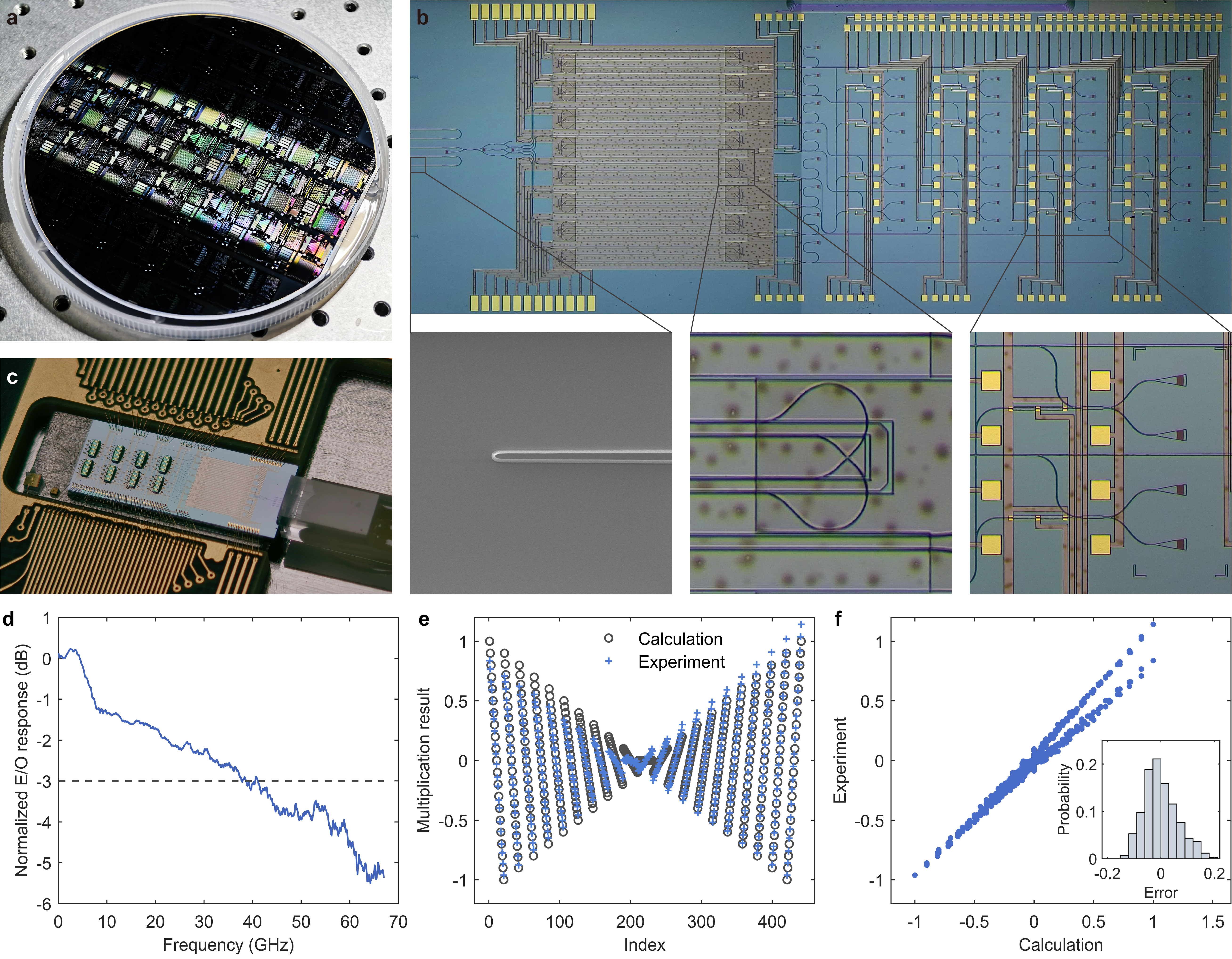
Figure 2: Fabrication and characterization of the HPTC chip, including wafer-scale process, packaged device, modulator frequency response, and analog computation benchmark results.
Electro-optic measurements revealed a -3 dB bandwidth of 37.8 GHz for the modulators, suitable for high-speed AI workloads. Analog computation accuracy was quantified via a 21x21 multiplication-table benchmark, which demonstrated robust linearity with a standard deviation error of 0.0621 in the measured results, supporting practical real-valued tensor arithmetic.
- Interface and power scaling: The architecture reduces the number of required high-speed electro-optic and ADC interfaces from O(n2) to O(n), a critical advance for large matrix sizes.
- Beam combining loss elimination: By leveraging local homodyne detection and temporal accumulation, the architecture avoids the severe optical loss penalties in spatial crossbar systems, converging the optical power scaling from O(n)0 to O(n)1.
- Integration density: The prototype achieves high integration density, with compact folded modulators and efficient vertical coupling.
- Analog computation accuracy: Experimental benchmarks demonstrate that real-valued matrix multiplications (outer products followed by accumulation) exhibit low error (standard deviation 0.0621), supporting high-fidelity analog photonic compute.
- Modulation bandwidth: The 37.8 GHz EO bandwidth supports current and near-future photonic compute workloads, particularly in AI matrix operations.
The architecture enables dynamic, high-speed updates of both data and weights at scale without ballooning interconnect or power requirements, a shift in the system bottleneck for photonic AI processors.
Implications and Future Directions
The HPTC concept evidences that photonic AI tensor accelerators can be designed to scale—the elimination of quadratic interface overhead and beam combining losses directly addresses critical bottlenecks at the system level. This unlocks the practical integration of large-scale photonic matrix processors for bandwidth-intensive, low-power AI workloads not only in data centers but also in edge and embedded applications where power and interface resources are particularly constrained.
Practically, the architecture can map high-dimensional, large-parameter AI models by supporting rapid, on-chip updates and high-throughput vector-matrix operations. The generality of time-domain accumulation also facilitates extension to temporal and recurrent computation primitives.
Theoretically, this shift in scaling could motivate new AI algorithms tailored to photonic co-design—those that exploit outer-product and time-integrated accumulation semantics, and algorithms tolerant to analog computation noise in exchange for bandwidth and energy efficiency.
Future research may address the extension to larger array sizes, further reductions in analog computation error (e.g., via device variation compensation), and integration of higher-order nonlinearity for nontrivial AI activation functions. Additionally, co-packaging of electronics for local control and further photonic–electronic interface optimizations will be crucial.
Conclusion
This work demonstrates a scalable, hardware-efficient homodyne photonic tensor core that fundamentally advances the architectural, integration, and operational paradigm of on-chip photonic AI processors. By reducing interface complexity to O(n)2, eliminating beam combining loss, and supporting real-valued, high-speed matrix computation with low error, the HPTC architecture constitutes a solid foundation for future high-bandwidth, energy-efficient photonic AI hardware (2606.16150).

