- The paper reveals that digital neuromorphic architectures continue to face an on-chip memory wall due to inefficiencies in SRAM and STT-MRAM technologies.
- The paper quantitatively analyzes energy–area trade-offs across register files, SRAM, and MRAM at 22nm nodes, highlighting significant design constraints in distributed memory systems.
- The paper demonstrates that severe mapping inefficiencies lead to low memory utilization and increased energy costs, underscoring the need for a holistic, co-designed memory architecture.
Memory Wall is not Gone: A Critical Evaluation of Memory Architecture in Digital Neuromorphic Computing
Introduction
Despite shifting computational paradigms from von Neumann to distributed neuromorphic architectures, the anticipated dissolution of the memory wall has not materialized in digital neuromorphic processors. While neuromorphic systems draw from the distributed memory organization observed in biological neural circuits, the instantiation of this principle in CMOS-based hardware exposes new scaling bottlenecks. The transition from energy-intensive off-chip memory accesses to area- and energy-constrained on-chip storage introduces a novel memory wall. The dominant energy and area costs associated with modern SRAM and emerging STT-MRAM blocks are demonstrated to subsume those of compute, subverting claims that neuromorphic architectures fundamentally sidestep the limitations inherent to conventional architectures.
Energy–Area Trade-offs in On-Chip Memory
The paper provides a rigorous analysis of mainstream memory technologies at advanced nodes. Three classes—register-based (RF), SRAM, and STT-MRAM—illustrate nonlinear scaling trade-offs between access energy and area density.
The empirical data at 22nm FDX nodes underscore the key architectural dilemma: small, distributed register files minimize access energy but suffer extreme area inefficiency, driving high leakage and limiting integration. Conversely, highly dense MRAM drastically reduces area per bit but exhibits high dynamic energy for both reads and (particularly) writes, which renders it unsuitable for frequent access patterns.
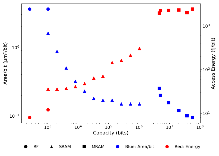
Figure 1: Energy-area trade-offs of Register Files (RF), SRAM, and MRAM at the FDX-22nm node illustrate the regime where SRAM and MRAM dominate both die area and energy.
While neuromorphic system design aspires to spatially distribute memory/compute (mimicking biological systems), the fragmenting of on-chip memory into many small blocks is fundamentally constrained by peripheral overheads, exacerbating die area and static power.
Impact of Distributed Architectures
Digital neuromorphic processors spatially couple small memory banks with processing elements (PEs), providing a structural basis for minimizing data movement. However, unlike compute—which is highly time-multiplexed—neuron state and synaptic parameter storage exhibit poor temporal reuse, requiring high parallelism and redundancy in physical memory. The result is that over 80% of die area is often dedicated to memory, with power profiles dominated by both dynamic accesses and static leakage.
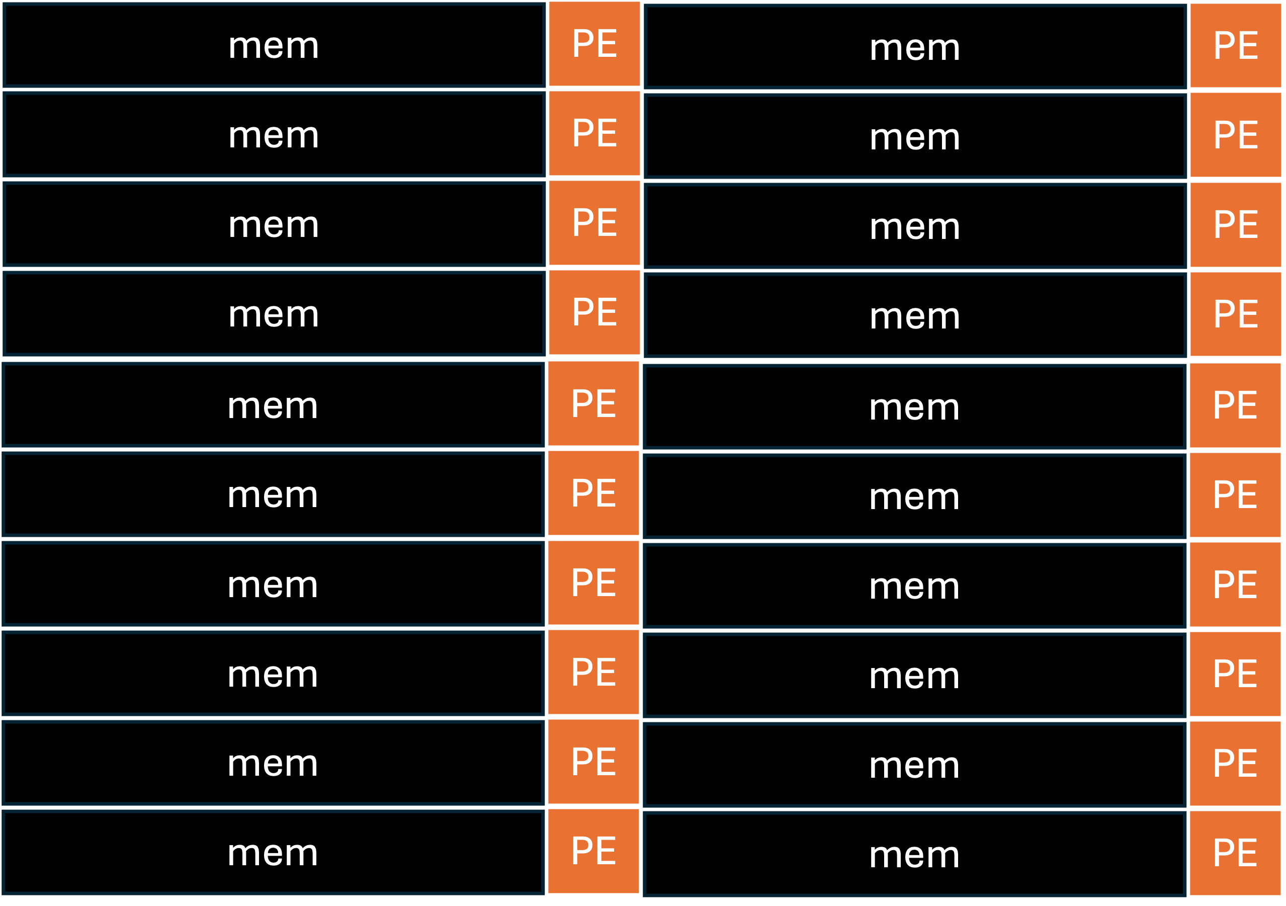
Figure 2: Distributed memory and processing elements in neuromorphic architectures are designed to eliminate the memory wall, but in practice shift the bottleneck on-chip.
Designers encounter a central compromise: decomposition into highly granular tiles increases the cost and energy of core-to-core communication and mounting leakage, while consolidating into large macro blocks raises dynamic energy for each memory access and leads to suboptimal mapping of network layers.
Neural Network-to-Hardware Mapping Inefficiency
Hardware-level mapping inefficiencies severely degrade effective memory utilization in state-of-the-art systems. Empirical data reveal that only 0.5%–30% of available on-chip memory stores useful network parameters in leading designs, with highly distributed chips (e.g., IBM TrueNorth, Intel Loihi) exhibiting utilization below 1%. The key causes are core size granularity mismatch with network layer dimensions, the need for persistent high-precision neuron state storage—unlike transient partial sums in conventional DNN accelerators—and intrinsic memory fragmentation.
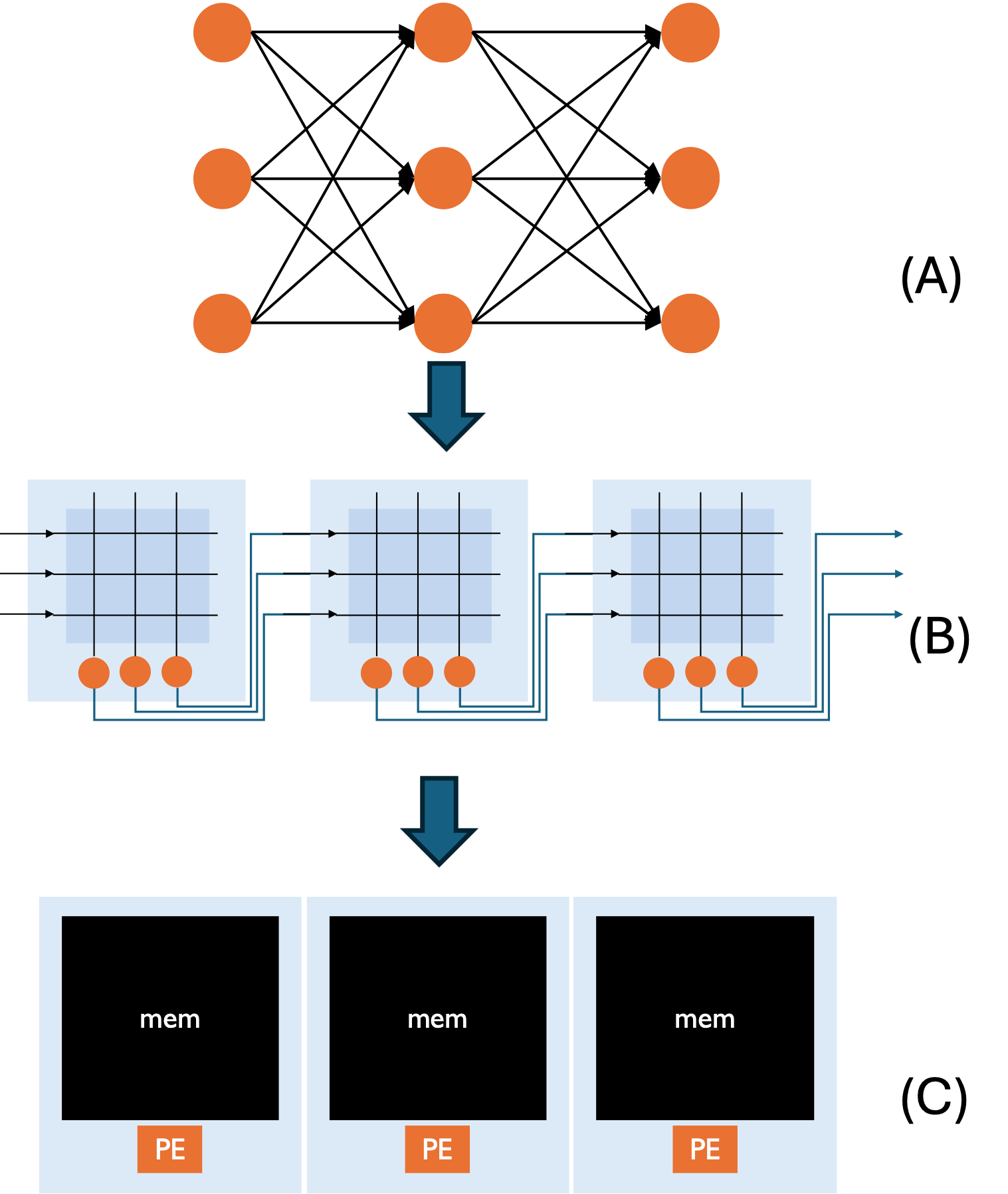
Figure 3: Spatial mapping of neural network layers onto tiled memory-processing element cores exposes unresolvable fragmentation and load imbalance, significantly reducing memory utilization.
This mapping inefficiency not only results in ‘dark silicon’ but also amplifies spike routing energy, as communication overheads escalate with low utilization and distributed mappings.
Pathways and Implications for Overcoming the Memory Wall
The persistent on-chip memory wall compels a comprehensive re-evaluation at the algorithm, software, architecture, and technology stack levels:
- Algorithmic adaptations: Hybrid networks employing a selective mix of stateful and stateless layers can sharply reduce persistent memory requirements, relaxing the all-stateful SNN constraint where temporal expressiveness is less critical.
- Software-level optimizations: Techniques such as spike grouping, event batching, and memory scheduling improve temporal and spatial locality, offering partial respite from bandwidth bottlenecks.
- Heterogeneous/hierarchical memory architectures: Integrating multi-tiered memory—hot data in low-energy register files, weights in SRAM, and infrequently accessed parameters in MRAM or RRAM—can enable joint optimization of energy and capacity, but introduces mapping and cost complexity.
- In-memory compute: MRAM/RRAM-based in-memory multiplication (crossbar arrays) can localize energy consumption, but mapping rigidity and the requirement for high-precision accumulator state outside memory arrays fundamentally limit the attainable energy savings and flexibility.
- 3D monolithic integration: Stacking NVM over logic enables large distributed memory without expanding silicon footprint. However, systematic penalties of non-volatile technologies—write latency, endurance, energy—persist, and the hierarchical architectural challenge remains.
Critically, the paper argues that piecemeal fragmentation or macro scaling does not erase the fundamental trade-off, and the majority of published benchmarks are tailored to fit hardware limits rather than exercising unconstrained AI workloads.
Conclusion
Digital neuromorphic architectures have not resolved the memory wall; rather, energy and area bottlenecks have moved on-chip, primarily due to the architectural overheads in current memory technology and organization. Mapping inefficiency, compounded by the interplay of memory and interconnect, renders many designs suboptimal, with pronounced implications for edge and embedded deployments. Future efforts must eschew incremental approaches in favor of jointly rethinking neuron models, mapping paradigms, and heterogeneous memory hierarchies. Theoretical advances in algorithm–hardware co-design and technology scaling, particularly in in-memory compute and 3D integration, offer partial but not complete solutions. If neuromorphic processors are to realize their claimed potential, a systematic abandonment of conventional memory architectures is imperative.