- The paper introduces a novel subthreshold SRAM-based compute-in-memory architecture that embeds distributed voltage regulators and current sensors to achieve PVT resilience.
- It demonstrates a 260× reduction in operating current, 87% static leakage savings, and a 43% reduction in bitcell output variability through innovative analog-domain techniques.
- The co-design with programmable neuron thresholds and stride-tick batching dramatically minimizes storage overhead and maintains high SNN inference accuracy (up to 93.64%).
PVT-Resilient Subthreshold SRAM-Based In-Memory Accelerator for Energy-Efficient SNNs
Introduction
The paper presents a CMOS-based, subthreshold-operating SRAM compute-in-memory (CIM) macro that is resilient against process-voltage-temperature (PVT) variations and optimized for energy-efficient spiking neural network (SNN) inference (2605.00319). By integrating in-situ current sensors and distributed voltage regulators directly within a large-scale SRAM array, the architecture allows robust, large parallel dot-product operations operating in the subthreshold regime, a context where most prior works encounter severe nonlinearities, reliability loss, or prohibitive power overheads. Additionally, the system employs a CIM- and SNN-specific co-design, including programmable, memory cell-based neuron thresholds and a stride-tick batching dataflow to maximize energy efficiency and reduce intermediate storage. Fabricated in a 28 nm process, the accelerator demonstrates notable energy and area efficiency while maintaining high task accuracy under aggressive voltage scaling.
Circuit Innovation for PVT Resilience in Subthreshold CIM
Traditional current-mode SRAM-based CIM macros are fundamentally challenged by variability in device characteristics, voltage supply fluctuations, and temperature-induced parameter shifts—all of which are exacerbated in subthreshold operation where device characteristics become strongly nonlinear or unpredictable. The proposed architecture adopts 8T SRAM cells, separating read/write accesses to enable robust parallel wordline activation without data disturbance. Unlike prior methods that address PVT drift via costly digital calibration or replica-based reference columns, the presented approach embeds distributed voltage regulators and on-chip PVT sensors. These monitor sensors dynamically regulate the local cell supply in each array segment to maintain a stable per-cell current reference regardless of environmental drift.
After the introduction of this regulation, simulated results show the SRAM bitline current (IRBL) is held constant over a wide temperature span, while operation at an aggressively reduced supply voltage (∼0.29 V) suppresses static power and limits signal overdrive, enabling high-density array operation simultaneously across 1,024 wordlines and 1,304 bitlines.
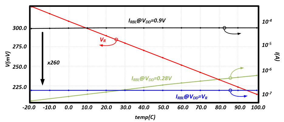
Figure 2: Simulated read bitline current in the regulated subthreshold SRAM macro demonstrates marked invariance over temperature, compared to unregulated and constant low supply baselines.
Notably, this approach achieves a 260× reduction in operating current compared to nominal voltage, with 87% static leakage savings, and delivers a 43% lower standard deviation in bitcell output current as validated by Monte Carlo simulations across process corners. The area overhead for this analog-domain correction measures under 2%, and the power penalty for threshold current generation is a mere 0.9% of overall chip consumption.
SNN-Focused Hardware-Software Co-design
The macro implements neural integration and spike generation within distributed neuron blocks. Each neuron leverages replica SRAM-based function cells to generate a programmable threshold current (ITH), directly controlling spike firing within process- and temperature-robust limits. The neuron architecture, operating in current-mode, accumulates input-weight product currents onto capacitors, triggering spike generation by a comparator circuit upon reaching the adjustable threshold.
The architecture supports 1–3 integration timesteps per inference, with temporal flexibility matched to application-level accuracy/latency trade-offs. A stride-tick batching scheme, which has strong roots in prior pipelined processing for SNNs but is here tailored with multi-line buffer partitioning, allows all timesteps for a block to be computed in sequence before moving to the next. This dramatically reduces the storage requirement for intermediate membrane potentials: for the presented keyword spotting SNN, the proposed dataflow brings buffer overhead down from 1488 Kb to 0.375 Kb (99.97% reduction).
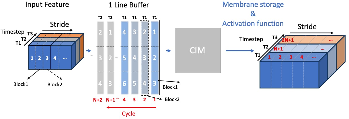
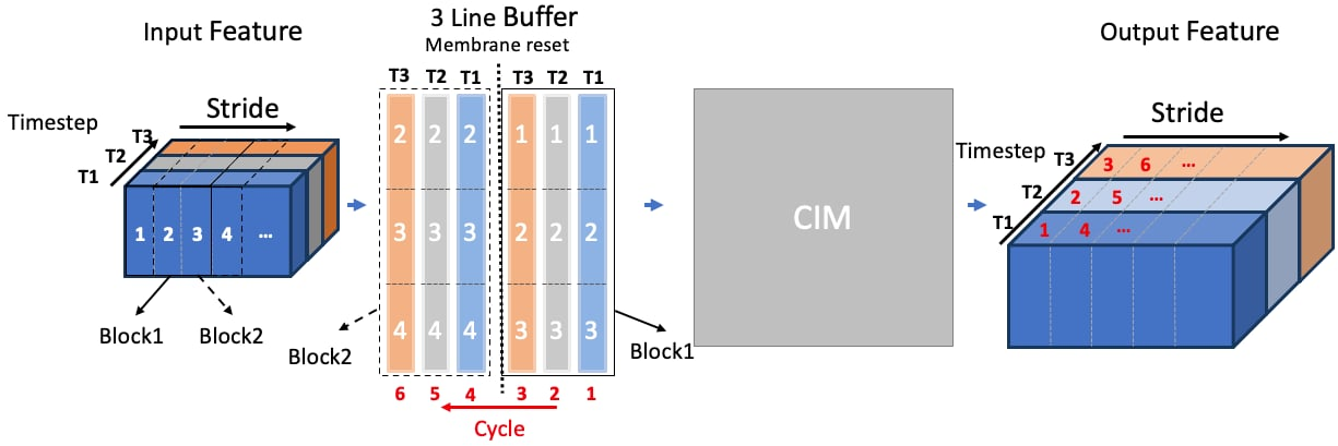
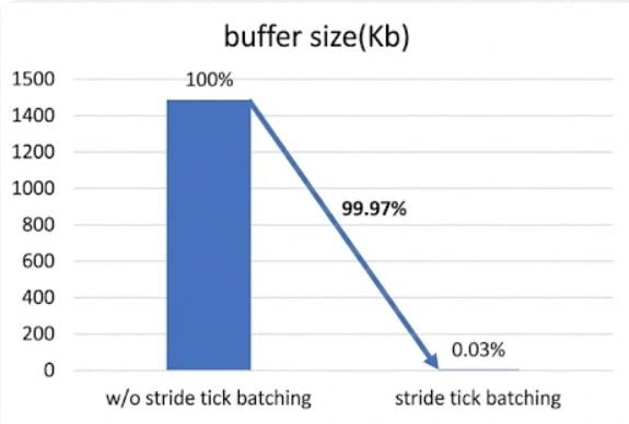
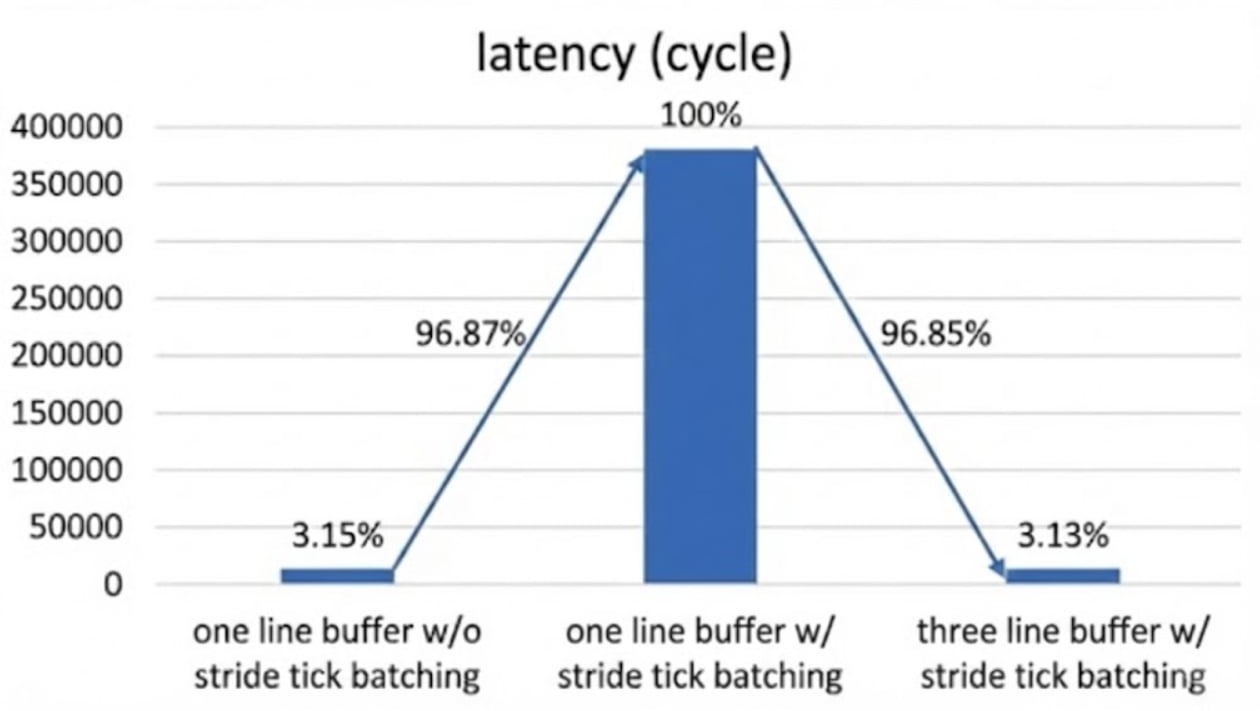
Figure 4: Dataflow schematic for stride-tick batching in the SNN CIM macro, depicting per-timestep buffering for high input reuse and minimized membrane state storage.
By distributing three line buffers—one per timestep—the architecture increases feature reuse (up to 66% in 3-timestep mode) and avoids throughput losses, balancing the overhead of the extra buffers against significant latency and storage gains.
Variation-aware training, using extracted SRAM and sense amplifier non-idealities from circuit-level Monte Carlo, is applied to refine model weights and improve robustness. This strategy allows the trained model to recover substantial accuracy lost to offset and noise, achieving 93.64% on GSCD and 85.59% on CIFAR-10, even in the presence of aggressive PVT and quantization effects.
Silicon Results and System Benchmarking
The chip, fabricated in 28 nm CMOS and area of 3.28 mm², contains 1.27 Mb of subthreshold 8T SRAM and 128 neuron instances with in-situ current sensors and distributed voltage regulation. Characterization across a 0.29–0.9 V supply range confirms reliable subthreshold inference, with a minimum operating voltage of approximately 0.29 V in CIM mode and a reduction in total chip power by 40% compared to traditional approaches.
Performance analytics demonstrate:
- Peak energy efficiency of 1181.42 TOPS/W (one-timestep SNN on GSCD), normalized to single-bit operation.
- Area efficiency of 7.24 TOPS/mm².
- Measured inference accuracy of 93.64% (GSCD, three timesteps) and 85.59% (CIFAR-10).
- Buffer overhead for membrane storage reduced by three orders of magnitude via the introduced dataflow.
When benchmarked against leading analog/mixed-signal CIM accelerators (RRAM, eDRAM, 6T/8T SRAM) in similar technology nodes, this system delivers an order-of-magnitude improvement in energy efficiency, operational at substantially reduced voltages and with robust tolerance to PVT variability.
Implications and Future Developments
This work demonstrates the viability of large-scale, subthreshold SRAM-based current-mode CIM for SNNs under realistic environmental stressors. By embedding physical-layer regulation for PVT resilience and enforcing hardware-software co-optimizations (including stride-tick dataflow, aggressive quantization, and variation-aware training), the proposed system breaks the bottleneck of reliability and energy scalability that has historically limited subthreshold CIM deployment.
The approach positions subthreshold 8T SRAM as a promising platform for near-memory computation in edge AI scenarios, particularly where ultra-low-power operation and dense deployment are required. The integrated system does, however, necessitate careful circuit-model-aware training and a hardware architecture tailored to SNN sparsity and temporal computation patterns.
Looking forward, the integration strategy could be generalized for even larger-scale models, and extended to multi-core or heterogeneous CIM systems. Opportunities also exist in adapting the physical regulation technique to even more advanced nodes or alternative memory cells (e.g., STT-MRAM or emerging non-volatile memories), and in further reducing the analog biasing and regulation overhead via streamlined sensor/regulator design. The demonstrated co-design methodology also paves the way for more sophisticated logic-in-memory schemes for spiking and possibly mixed ANN-SNN hybrid workloads.
Conclusion
The presented architecture achieves robust, PVT-resilient inference for SNNs through a synergistic melding of circuit-level voltage regulation and algorithm-level training. The embedded current sensors and distributed regulators ensure operation deep into the subthreshold regime, while the dataflow and neuronal threshold schemes eliminate key overheads found in prior CIM accelerators. Achieving state-of-the-art energy/area efficiency and strong task accuracy, this work sets a concrete footing for future developments in ultra-low-power neuromorphic and edge AI processing.

