- The paper demonstrates that training DLGNs with a silicon-aware loss reduces average gate area while maintaining high classification accuracy on datasets like MNIST.
- It details a methodology for directly mapping discrete, differentiable logic gate networks onto CMOS standard cells, achieving ultra-low inference latency and high throughput.
- Empirical results highlight trade-offs between accuracy, area, and power, underscoring the potential for efficient edge AI deployments.
Silicon Aware Neural Networks: DLGNs Synthesized for CMOS Implementation
Overview
"Silicon Aware Neural Networks" (2604.19334) investigates the direct mapping of Differentiable Logic Gate Networks (DLGNs) trained for image classification onto digital CMOS hardware, with specific attention to process-aware constraints such as standard cell area and overall power efficiency. The authors propose a novel area-aware loss function to guide DLGN training for improved silicon utilization and demonstrate, via layout and post-layout analysis in the SkyWater 130nm node, that logic gate-based models can be both functional and highly efficient as ASIC macros.
Differentiable Logic Gate Networks: Architectures and Training
DLGNs depart from traditional neural network architectures by representing neurons as compositions of two-input logic gates rather than matrix multiplications or dot products. Each node can choose among 16 Boolean logic functions (e.g., NAND, OR, XOR), with the selection optimized during training. To circumvent issues of non-differentiability, the architecture relaxes logic gates to continuous approximations and probabilistically selects gates via softmax. Discrete assignments are made post-training.
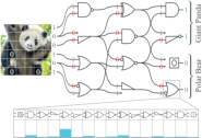
Figure 1: Conceptional visualization of a DLGN for image classification, as introduced in Convolutional DLGNs.
This construction allows DLGNs to directly utilize discrete logic, lending themselves naturally to digital standard cell-based synthesis. However, in a real silicon context, the area and power consumption of CMOS gates differ significantly by type. For instance, NAND gates are more compact and efficient than XOR gates. As such, silicon-aware optimization is necessary for practical implementation.
Area-Aware Loss for Hardware Optimization
The paper introduces a hardware-aware empirical risk minimization objective by augmenting classical cross-entropy loss with a differentiable area penalty. The expected area per neuron is computed by weighting the area of each possible logic gate by the softmax-derived probability of its selection:
E[arean]=pn⊤A
where A comprises the known or estimated areas for each gate mapped to standard cell implementations in the reference library (SkyWater 130nm/Cadence). The total loss is:
Ltotal=LCE+δ⋅Larea
where δ controls the trade-off. Empirically, δ=0.01 minimized area without significant degradation in classification accuracy, with stable convergence observed across training.
Direct Mapping and ASIC Layout in SkyWater 130nm
Upon training a DLGN with area-aware loss, the model's logic is discretized and mapped straightforwardly to Cadence SkyWater 130nm standard cells. Practical issues such as unbalanced logic mapping and limited routing in 1P5M CMOS require architectural adaptations; the design used 18 layers of 4,000 neurons per layer, finding this configuration tractable for silicon realization at the chosen process node.
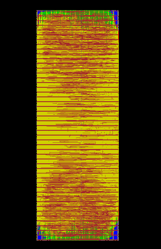
Figure 3: Complete post-layout design of a DLGN hard macro in SkyWater 130nm, suitable for custom ASIC instantiation.
Functional verification was performed through gate-level simulation, and subsequent Innovus placement and routing yielded a hard macro ready for power and timing analysis. The implementation efficiently mapped GroupSum aggregation (used for class logits) to popcount binary adder trees using standard cell adders.
Empirical Results: Accuracy, Area, Latency, and Power
On MNIST, the DLGN realized in standard cells retained a classification accuracy of 97%, while achieving an average gate area of 6.1 μm² per neuron with the area penalty (down from 9.4 μm² baseline), for a total logic area of 1.95 mm². For CIFAR-10, a trade-off between accuracy (~59%) and average area per neuron (~7.5 μm²) was also observed.
The hard macro demonstrates ultra-low inference latency and high throughput, measured at a worst-case delay of 23.9 ns, translating to 41.8 million inferences per second on-silicon. Power analysis under high activity (70% input toggle) yields a total draw of 83.88 mW or 2.0 nJ per inference.
Process scaling using FO4 metrics enables fair comparisons with accelerators in more aggressive nodes. When normalized to a 16 nm process, the macro is projected to achieve 4.2 ns latency and 69 pJ/inference, demonstrating strong competitiveness or dominance over contemporaneous digital and mixed-signal edge AI designs.
Theoretical and Practical Implications
By enabling direct, loss-aware, gate-level mapping of neural networks, DLGNs open avenues for exploiting discrete logic function selection in hardware-aware neural model training. This stands in contrast to conventional approaches that require quantization, pruning, or laborious hand-off synthesis optimization steps. Furthermore, designing neural architectures inherently indifferent to the specific logic instantiations at each neuron enables joint optimization of task accuracy and hardware cost, allowing for more aggressive area, power, and possibly leakage optimization by neural model search.
On the practical side, this methodology lowers the barrier to creating application-specific AI macros for edge deployment, where area and energy budgets are highly constrained. Open PDKs such as SkyWater 130nm, together with public standard cell libraries, facilitate transparent evaluation, repeatability, and further co-design innovations at the model-architecture-process intersection.
Future Directions
The work suggests the direct path to silicon tapeout and experimental prototyping, with the possibility of real-world validation of power and error rates under process variation and noise. Extending the framework to more advanced nodes and exploring even tighter model-process coupling (e.g., including routing or wire energy in the loss, or exploiting process-specific cell availability) are logical progressions. Furthermore, the approach could inform a broader class of model-based digital design flows where logic ambiguity is resolved dynamically for optimal PPA metrics.
Conclusion
This work demonstrates that DLGNs, when trained with silicon-aware objectives, can be mapped efficiently and effectively to standard cell ASICs using modern open CMOS processes, achieving strong accuracy, throughput, and energy efficiency. The results support further exploration of hardware-aware neural network co-design as a direct path to low-power, high-speed edge inference accelerators.