- The paper presents a high-yield method for fabricating concave silica micromirrors via feedback-controlled CO₂ laser ablation.
- It integrates real-time white-light emission monitoring and interferometric positioning to reduce depth variance from 10% to 3% and achieve precise curvature control.
- The technique enables scalable production of high-finesse microcavities, supporting advanced applications in quantum electrodynamics and optomechanics.
High-Yield Fabrication of Micromirror Templates via Feedback-Controlled Laser Ablation
Introduction and Motivation
The fabrication of concave micromirror templates in silica substrates is foundational for the realization of high-performance microcavities, with applications spanning cavity quantum electrodynamics (QED), quantum information, and cavity optomechanics. Traditionally, micromirrors in silicon have been produced via etching, but silica offers advantages due to its low optical absorption and broad transparency window. Laser ablation with a focused CO₂ beam enables micrometer-scale, ultra-smooth concave structure formation, crucial for low-loss, high-finesse optical resonators. However, key challenges persist: mitigating geometric variability and asymmetry, achieving reliable one-shot fabrication on valuable substrates, and tailoring mirror geometry for scalable cavity integration.
This work presents an automated, high-yield method for fabricating concave micromirrors using feedback-controlled CO₂ laser ablation, complemented by in situ interferometric sample positioning. Real-time white-light emission monitoring during ablation is used to precisely terminate laser exposure, suppressing variability in mirror depth and radius of curvature (ROC). The system incorporates an integrated phase-scanning interferometric microscope for sample localization, facilitating reproducible processing across substrates.
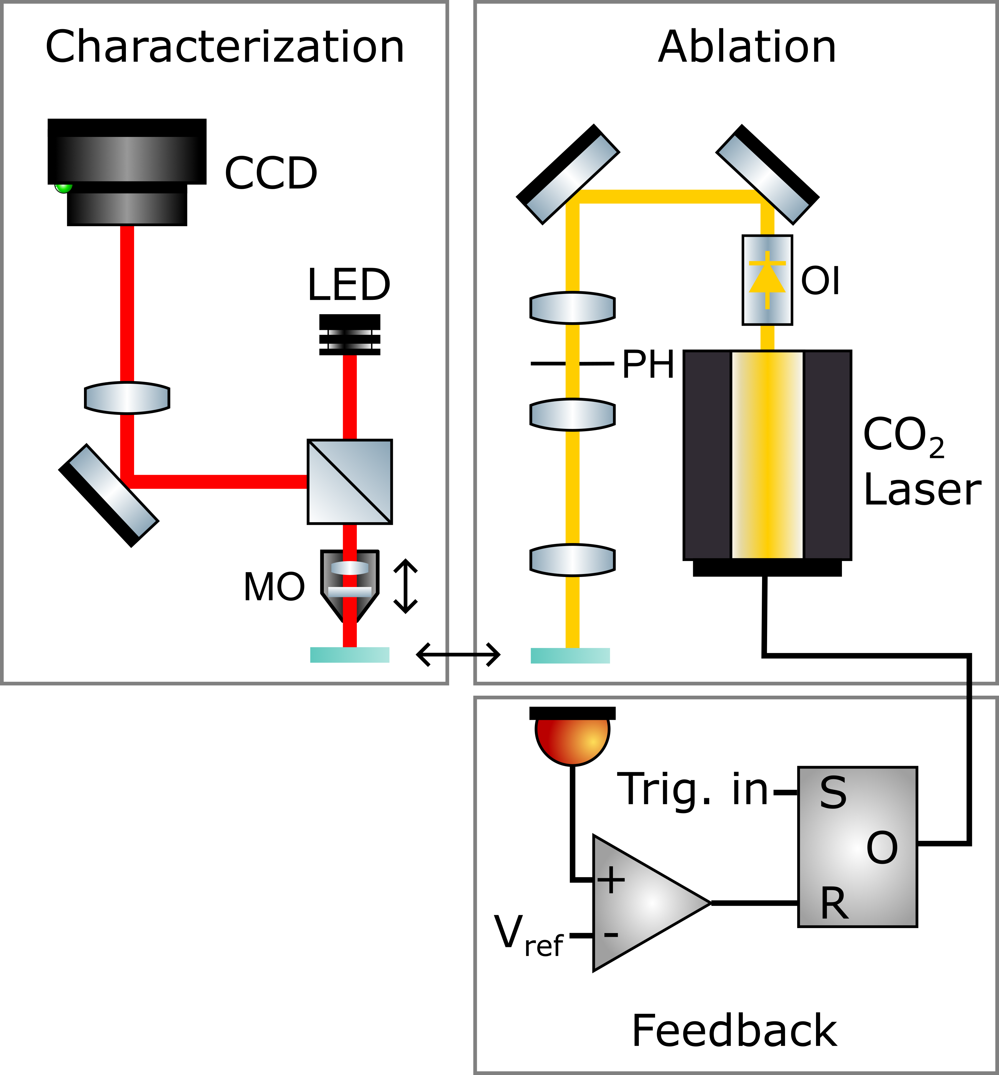
Figure 1: Schematic of the mirror fabrication setup with integrated interferometric sample positioning and motorized translation between ablation and characterization stations.
Experimental Setup and Fabrication Process
The setup comprises two main components: a laser ablation station equipped with a mode-cleaned, focused CO₂ beam, and a characterization station implementing a phase-scanning interferometric microscope for topology reconstruction.
Laser Ablation with Feedback:
The CO₂ laser (10.6 μm, 40 W) is focused onto the substrate through a mode-filtered telescope terminated by a ZnSe lens. During ablation, white-light emission from the heated substrate is monitored with a silicon photodiode, whose voltage output serves as the feedback variable. An electronic circuit comprising a voltage comparator and SR latch triggers precise laser shutoff once the emission crosses a programmable threshold (Vref). This protocol robustly terminates ablation, abating variance originating from stochastic laser firing delays, optical alignment, or substrate heterogeneity.
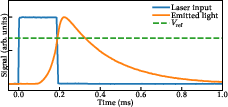
Figure 2: Time traces during ablation: laser modulation (blue), photodetector emission (orange), and shutdown threshold (dashed green).
Interferometric Sample Positioning:
Accurate localization of the substrate’s surface relative to the ablation focus is essential for geometric reproducibility. An in situ Mirau interferometric microscope, combined with a motorized 3-axis stage, enables autofocus and spatial alignment. Calibration experiments identify the focal position that minimizes the curvature asymmetry of the ablated features.
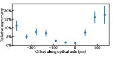
Figure 3: Relative curvature asymmetry as a function of sample offset along the laser axis, establishing optimal focal alignment for ablation.
Automated Workflow:
The complete workflow, integrated under a graphical user interface, cycles between sample characterization, translational alignment, single-shot feedback-driven ablation, and post-process topology assessment. Automated operation enables fabrication rates approaching one mirror per minute.
Characterization and Data Analysis
Surface Metrology:
Fabricated templates are characterized by phase-scanning interferometry, reconstructing their topography with ~100 nm lateral resolution. Features are modeled as elliptic paraboloids, characterized by depth, principal axes of curvature (Ra, Rb), and asymmetry parameter.
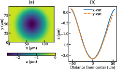
Figure 4: Height map and line profiles of a fabricated mirror template, demonstrating sub-micron dimensional control.
Suppression of Fabrication Variability:
A core result is the quantitative reduction of geometric spread through feedback control. A comparative study of 100 mirrors produced with and without emission-based feedback reveals a decrease in relative depth variance from 10% to 3%, and ROC variance from 6% to 3%. Feature asymmetry remains low (∼3%) in both cases, indicating that feedback primarily addresses ablation duration rather than focus-induced asymmetry. Histograms elucidate the non-Gaussian, positively skewed distribution of effective ablation times in the open-loop case. Feedback narrows this distribution and strongly correlates both feature depth and curvature with the actual ablation duration.
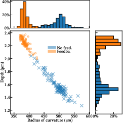
Figure 5: Depth and radius of curvature distributions of 100 micromirrors fabricated with (orange) and without (blue) emission-based feedback.
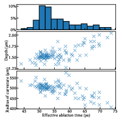
Figure 6: (Top) Effective ablation time histogram for open-loop process; (Middle) Feature depth vs ablation time; (Bottom) Radius of curvature vs ablation time.
Parameter Tuning and Geometric Range:
Geometric outcomes can be tuned via optical parameters (laser power, focal length) and feedback threshold (Vref). Using a 100 mm focusing lens (∼300 μm ROC), reduction of lens focal length to 25 mm enables ROC down to ∼20 μm. Systematic variation of Vref yields a broad parameter space in feature depth and ROC, replicating established power-law relationships between these variables.
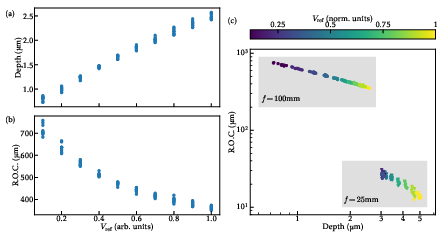
Figure 7: Dependence of mirror depth and radius of curvature on the feedback threshold Vref, showing tuning capability over a broad geometric range.
Application: High-Finesse Microcavity Demonstration
Cavity Assembly and Optical Testing:
To assess suitability for practical devices, a plano-concave Fabry–Perot microcavity is constructed employing a fabricated concave silica mirror (ROC ≈ 270–300 μm) and a planar silicon mirror, both coated with low-loss dielectric DBRs. The fixed-length cavity (∼71 μm) demonstrates high finesse (F=3.7×10⁴ at 1568 nm), with negligible birefringence-induced mode splitting.
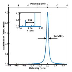
Figure 8: Transmission spectrum of the assembled microcavity, showing two resonances and a narrow fundamental linewidth indicative of high finesse.
This performance attests to the low surface roughness and geometric precision achievable with this method and establishes the applicability for QED and optomechanical platforms requiring low-loss, high-cooperativity resonators.
Implications and Future Prospects
The integration of real-time emission feedback and precision in situ positioning constitutes a robust, scalable platform for micromirror fabrication in silica. The method’s reproducibility and yield (>97%) are highly advantageous for producing mirror arrays on patterned or pre-processed substrates, and are uniquely suited for applications requiring single-shot processing (e.g., phononic crystal mirrors for optomechanics (Allepuz-Requena et al., 15 Jan 2026)). Compared to multiplexed post-processed etching in silicon [wachter_silicon_2019], this approach matches or exceeds geometric control while leveraging the superior optical properties of silica.
The precise, automated workflow is extensible to arbitrary layouts for custom photonic integration, including directly atop planar photonic circuits [cheng_harnessing_2025], and is compatible with further advances in coating technology or geometric engineering (e.g., FIB-assisted ablation [33, Maier et al.]). The ability to reliably access ultra-small ROC enables access to sub-wavelength optical mode volumes relevant for strong-coupling CQED [gallego_strong_2018], and supports highly miniaturized optomechanical sensors or accelerometers.
Conclusion
This work establishes a high-throughput, feedback-controlled laser ablation platform for the fabrication of ultra-low-variance, low-roughness concave micromirrors in silica, verified via high-finesse microcavity implementation. The methodology enables scalable, automated production of tunable, application-optimized microcavities, supporting advances in cavity QED, cavity optomechanics, and integrated quantum photonics. Future expansions may include further automation, parallelization, and integration with nanoscale patterning to enable next-generation quantum and photonic devices.