- The paper demonstrates that negative-voltage biasing in 2D PeFET NVMs (NeVo HD and NeVo 2T-1P) significantly reduces bit-line energy, achieving up to 0.06× lower read energy.
- It details a novel architecture that couples a FE/PE capacitor stack with a monolayer MoS₂ transistor, exploiting strain-induced bandgap modulation for non-destructive readout.
- The study introduces efficient in-memory computing primitives—including single-cycle addition, subtraction, and STP-MAC for DNNs—that outperform conventional SRAM and earlier NVM designs.
Negative-Voltage-Enabled Energy Efficient Nonvolatile Memories and In-Memory Computing Based on 2D Piezoelectric Transistors
Introduction
This paper addresses the critical challenges limiting the scalability and energy efficiency of nonvolatile memories (NVMs) and in-memory computing (IMC) by leveraging 2D material-based Piezoelectric FETs (PeFETs). Prior PeFET NVM architectures exhibited a trade-off between integration density, energy efficiency, and IMC-compatibility, which constrained their applicability, especially in the context of data-intensive workloads and deep neural networks (DNNs). The authors propose two new PeFET-based memory designs—NeVo HD and NeVo 2T-1P—that employ negative-voltage (NeVo) biasing strategies to minimize the dominant energy components associated with bit-line charging, enabling simultaneously high density, low energy operation, and IMC support.
PeFET Device Structure and Mechanisms
PeFETs are constructed using a FE/PE (e.g., PZT-5H) capacitor stack coupled to a 2D transition metal dichalcogenide (TMD) transistor channel (e.g., monolayer MoS2), exploiting both the non-volatility of ferroelectric polarization and the strain-sensitive bandgap of the 2D channel. Bit storage corresponds to the polarization state of the FE, which can be manipulated via gate-to-back voltages (VGB), while readout exploits strain modulation in the 2D channel—expansion or contraction of the PE layer modulates the bandgap and consequently, channel current.
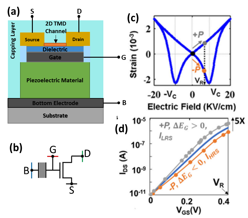
Figure 1: (a) PeFET device and (b) schematic. (c) Strain as a function of VGB exposes the strong electro-mechanical coupling exploited for non-destructive readout.
For accurate device modeling, a Preisach-based FE response is coupled with physical simulations of strain transfer and an S2DS-derived analytical TMD FET model that dynamically incorporates the bandgap modulation.
Analysis of Prior PeFET NVM Architectures and Their Limitations
Four principal PeFET NVM cells have been studied previously: the ultra-compact High Density (HD) cell, the 1T-1P with access gating, the cross-coupled (CC) configuration, and the 2T-1P enabling basic IMC. Each topology reflects a trade-off between density, functionality, and the parasitic energy cost of bit-line charging, with HD cells being optimal for density but poorer for write efficiency, and 2T-1P being IMC-capable but incurring greater area and bit-line energy penalties.
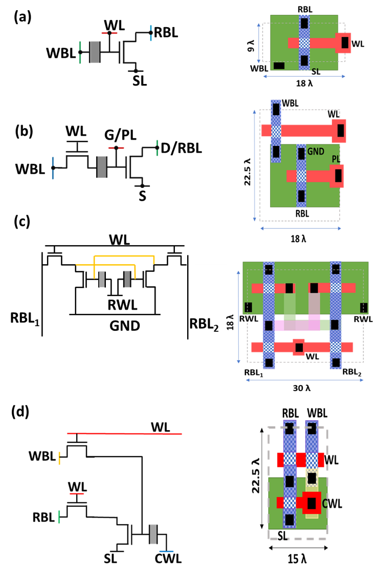
Figure 2: Schematic and layouts of PeFET NVM cells showing the array architectures: (a) HD, (b) 1T-1P, (c) CC, (d) 2T-1P.
Extensive energy analysis demonstrates (Figure 3) that the majority of read energy dissipation arises from charging parasitic-capacitance-laden bit-lines (RBLs and WBLs), a challenge exacerbated as array sizes scale.
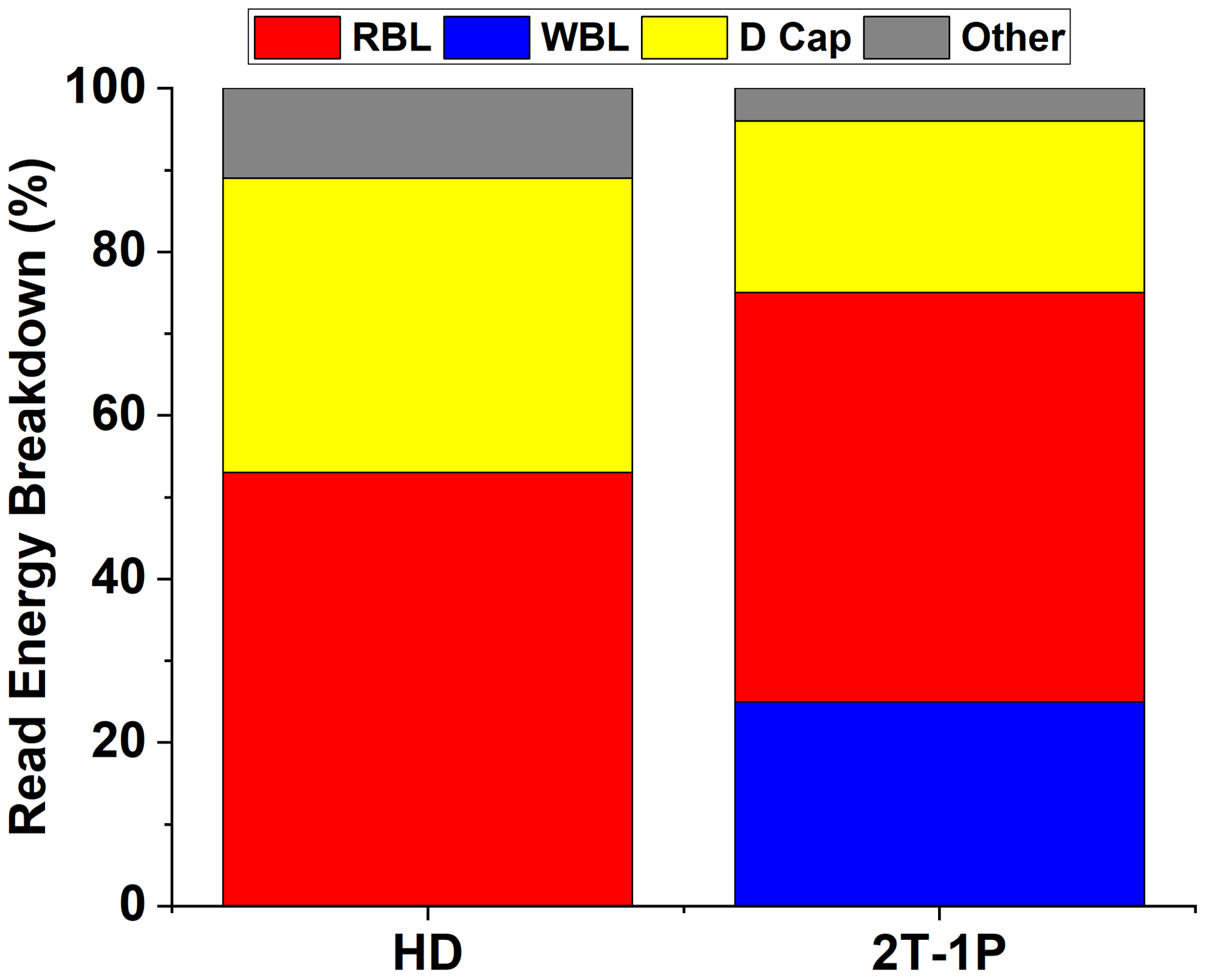
Figure 3: Decomposition of current-sensing read energy, showing bit-line and drain capacitance dominate for HD and 2T-1P NVMs.
NeVo HD and NeVo 2T-1P: Negative-Voltage-Enabled PeFET NVMs
Bit-Cell and Array Structure
NeVo HD retains single-PeFET simplicity but reorients array connections to permit negative voltage biasing on word-lines and source-lines, enabling parasitic-free bit-line operation. NeVo 2T-1P similarly reforms the biasing schema for 2T-1P, primarily targeting the elimination of vertical line charging overheads.
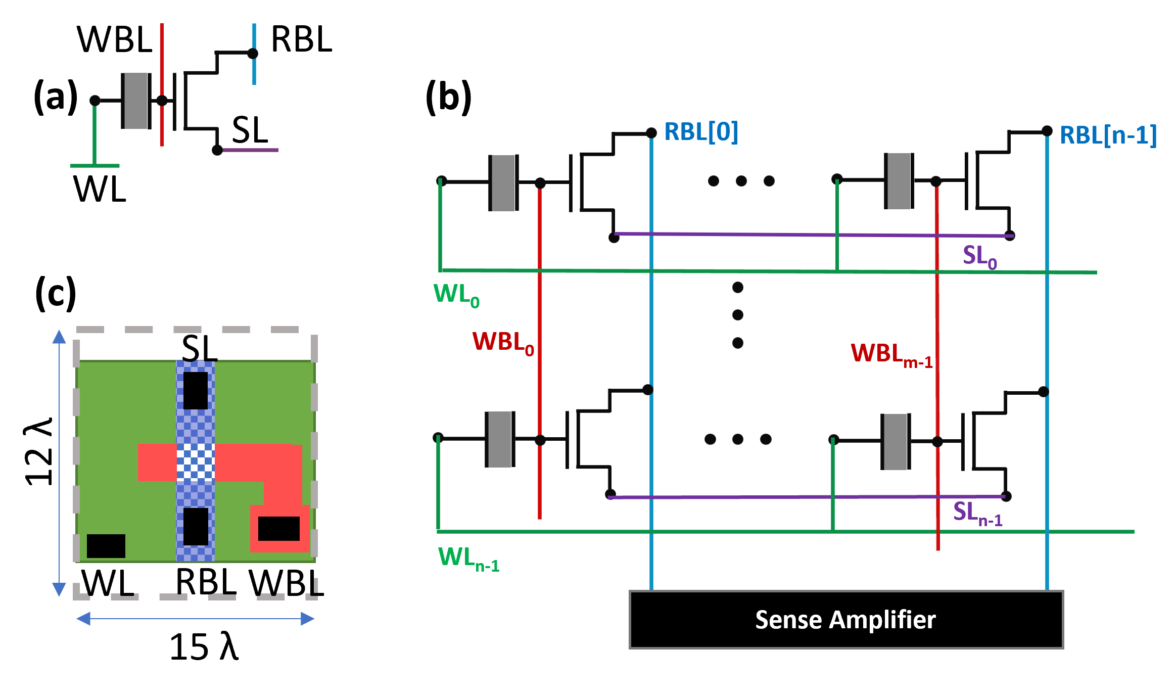
Figure 4: Schematics, array, and layout of NeVo HD, designed for negative-voltage-enabled energy minimization.
Read and Write Operations
Current-sensing read in the NeVo designs eliminates RBL charging by grounding RBLs and shifting the necessary biasing to horizontally routed lines. As shown in Figure 5, this modification results in 0.06× (NeVo HD vs. HD) and 0.03× (NeVo 2T-1P vs. 2T-1P) reduction in read energy, while write energy is reduced through minimized high-voltage swings and the limiting of PE charging to the targeted subset of capacitors.
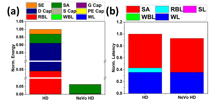
Figure 5: Demonstrates substantial current-based read energy and latency gains for NeVo HD relative to the HD cell.
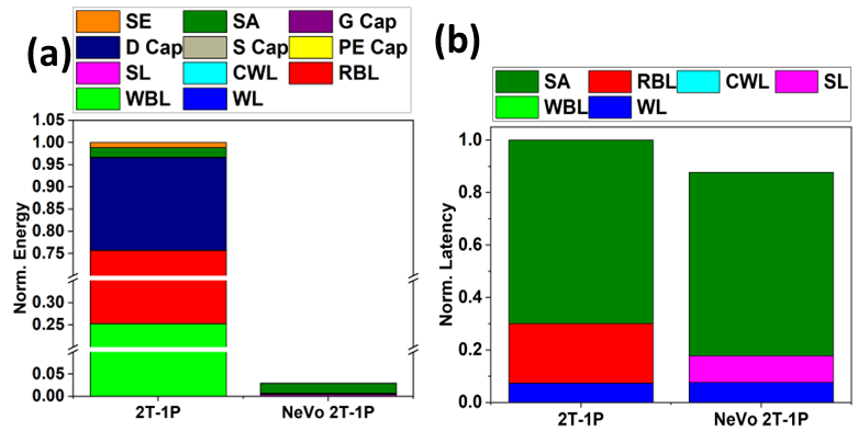
Figure 6: Read energy and latency improvements for NeVo 2T-1P compared to conventional 2T-1P cells.
Voltage-sensing read is less effective for NeVo HD due to increased leakage in grounded BL configurations and the necessity of precharging, but remains beneficial for NeVo 2T-1P. Write operation energy for NeVo 2T-1P is halved compared to 2T-1P, with a moderate latency penalty from reduced overdrive.
Comprehensive Benchmarking Versus Prior PeFET NVMs and SRAM
The authors benchmark NeVo HD and NeVo 2T-1P against SRAM, HD, and 2T-1P designs. NeVo 2T-1P achieves the highest read/write energy efficiency with 0.19× (read) and 0.55× (write) energy relative to 2T-1P, with NeVo HD offering the smallest cell area (0.19× SRAM). All NeVo designs outperform SRAM and previous PeFET NVMs in read energy per operation.
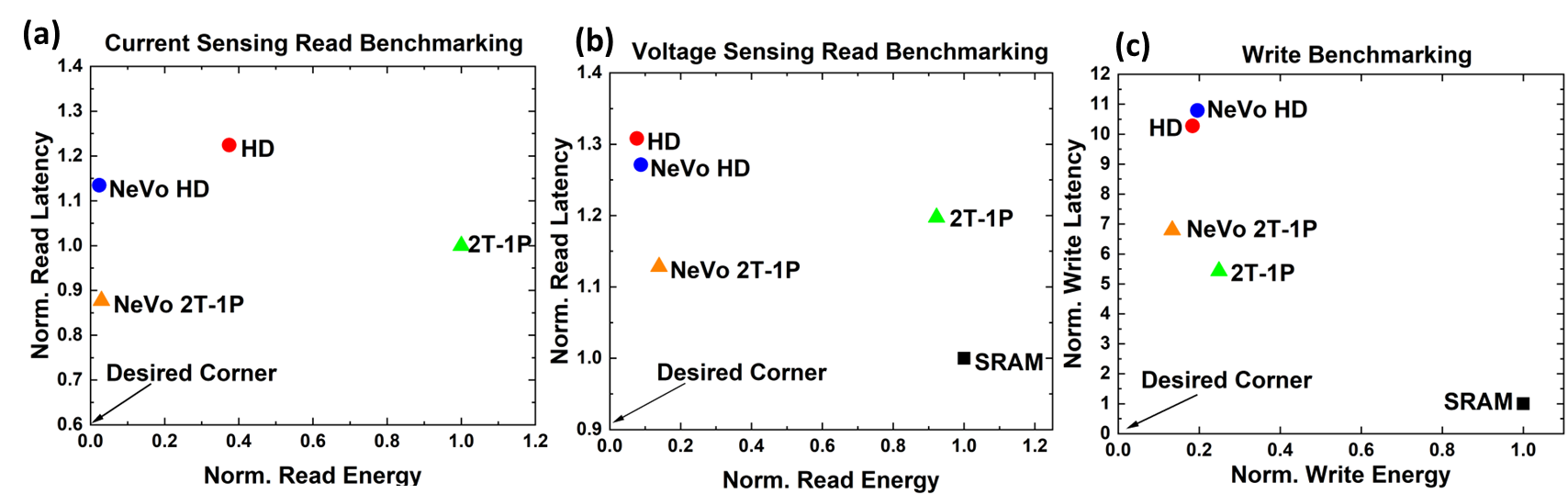
Figure 7: Comparative benchmarking of memory core operations across NeVo designs, previous PeFET cells, and 6T-SRAM.
In-Memory Computing Primitives: Enabling Efficient Addition, Subtraction, and Ternary MAC
The NeVo biasing approach, coupled with PeFETs’ unique polarization and VGB-polarity dependent transfer characteristics, is leveraged to realize low-energy, parallel in-memory addition, subtraction, and signed ternary precision multiply-and-accumulate (STP-MAC) primitives. Unlike prior approaches limited to commutative logic or multi-cycle computation, these operations employ simultaneous multi-row activation and current-mode analog summation, exploiting the full dual-polarity behavior of PeFETs.
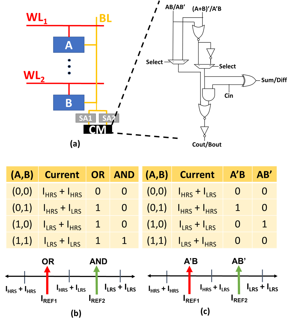
Figure 8: Architecture of IMC-capable memory array, facilitating direct addition and subtraction using dual SA and compute modules.
Energy and latency benchmarking (Figures 14 and 15) show NeVo cells achieve single-cycle, low-energy in-memory computation, with NeVo HD and NeVo 2T-1P reaching as low as 12% (NeVo HD, current-sensing) and 21% (NeVo 2T-1P, voltage-sensing) of the energy required by classic NMC approaches.
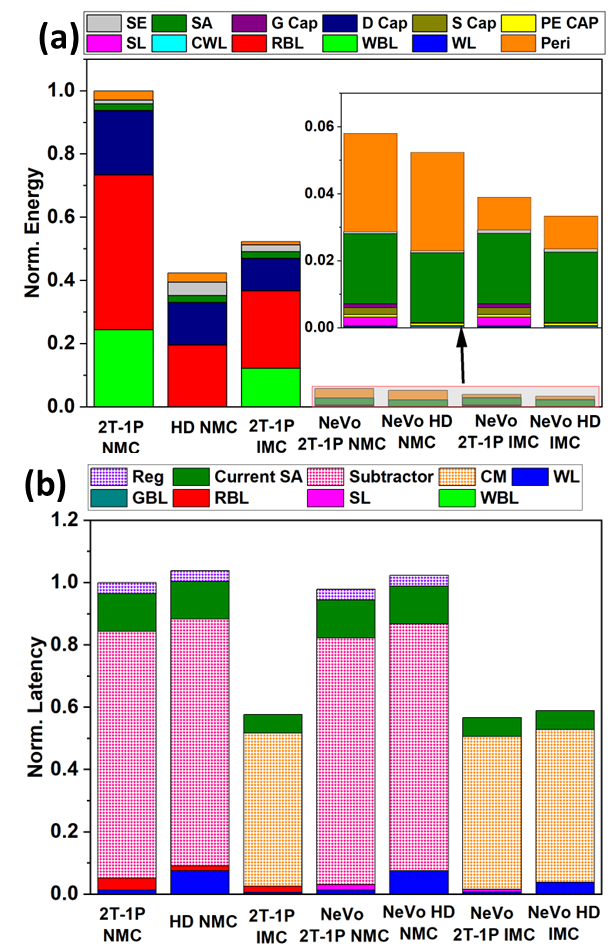
Figure 9: Current-sensing in-memory subtraction energy and latency comparisons highlight NeVo benefits.
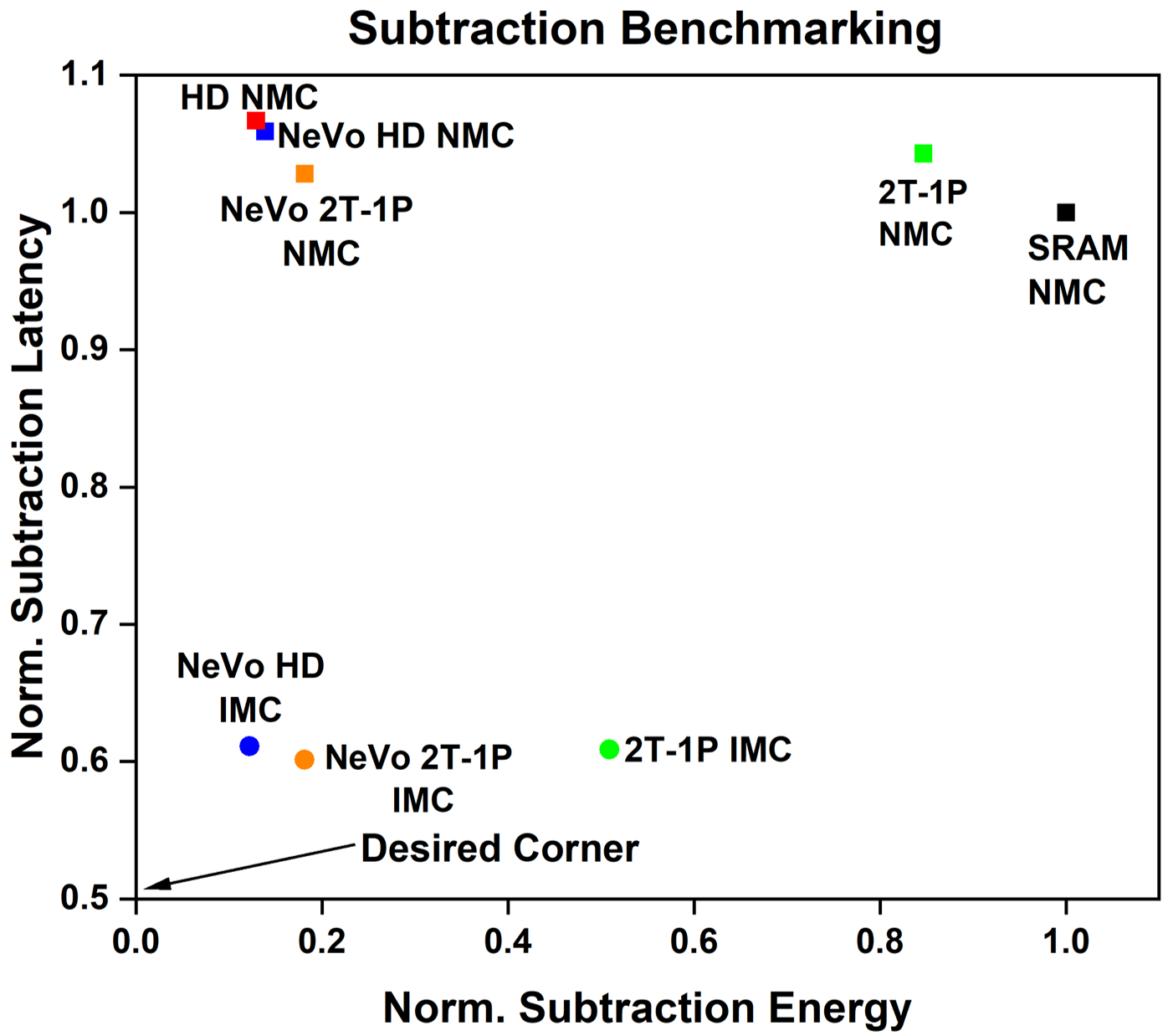
Figure 10: Voltage-sensing benchmarking of PeFET NVMs versus SRAM in subtraction operations, showing universal PeFET advantage.
STP-MAC Implementation and Optimization
For DNN-specific workloads, ternary multiply-and-accumulate is realized using double-PeFET mapping per weight, dual-polarity voltage supply for basis encoding, and parallel multi-row assertion to amortize ADC overhead. NeVo 2T-1P achieves 0.19× the energy of 2T-1P for MAC, permitting highly parallel analog compute within memory constraints, and NeVo HD further reduces energy cost through its more compact layout.
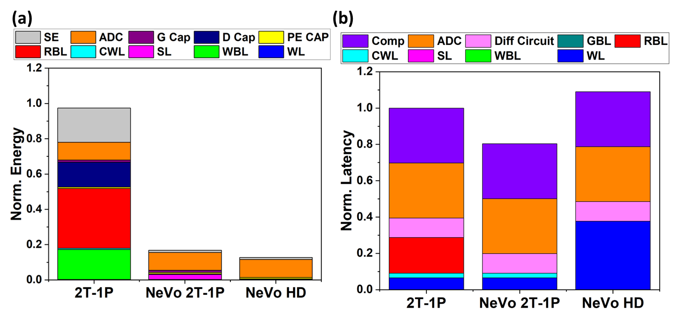
Figure 11: STP-MAC energy and latency: NeVo HD and 2T-1P set new state-of-the-art in efficiency.
Practical and Theoretical Implications
The presented NeVo design paradigm eliminates the persistent bit-line energy bottleneck in dense NVMs by enabling orthogonal control of cell biasing using negative voltage rails, a circuit-level innovation directly enabled by the PeFET device’s dual-mode electromechanical transfer characteristics. It further overcomes longstanding IMC limitations in performing both commutative and non-commutative functions (addition and subtraction) efficiently in memory and, uniquely, supports high-efficiency STP-MAC suitable for hardware ternary DNNs.
These results strongly motivate follow-on research in several directions:
- Process-Driven Scaling: The robustness of the NeVo approach with array-size scaling, device variability, and endurance requires experimental validation on large arrays and across process nodes.
- Architectural Co-Design: Integrating NeVo-based PeFET NVMs within real-system memory hierarchies and accelerator architectures will reveal trade-offs in overall system-level energy, latency, and PPA.
- Extension to Other 2D Materials: Leveraging alternate TMDs, or hybrid FE/PE stacks, could evolve the voltage/strain tunability further and potentially introduce additional IMC modalities.
- Device Reliability: Negative-voltage generation circuits and noise margins demand further investigation for robust and manufacturable system integration.
Conclusion
Negative-voltage-enabled PeFET NVMs (NeVo HD and NeVo 2T-1P) present substantial advances in the energy efficiency, density, and IMC capabilities of NVM technology. By architecting the cell and array for negative-voltage operation, this work establishes new reference points for both memory core energy and analog in-memory compute, directly addressing several of the most pressing limitations in high-density NVMs. The NeVo framework broadens the design space for 2D-material-based computation, and anticipates future memory-centric mixed-signal hardware for energy-constrained AI and conventional workloads.
(2604.03959)

