- The paper presents the first design and simulation of a superconducting qubit for the QUB-IT experiment using an Xmon configuration and the Qiskit-Metal toolkit.
- The paper utilizes Ansys Q3D and HFSS to extract key capacitance values, yielding a coupling strength of 47.38 MHz and a relaxation time of 13 μs.
- The paper demonstrates robust qubit-resonator interactions and QND measurement potential, paving the way for further optimization in quantum sensing.
Overview of the Design and Simulation of a Superconducting Qubit for the QUB-IT Experiment
The paper "First design of a superconducting qubit for the QUB-IT experiment" details the design and simulation of a transmon superconducting qubit coupled to a resonator. This paper contributes to quantum sensing, with specific focus on applications in Axion dark matter experiments such as QUAX, leveraging Quantum Non Demolition (QND) measurements and entangled qubits.
Design Methodology
The superconducting qubit design is executed using the Qiskit-Metal toolkit, underscoring the integration of modern software tools in quantum device development. The design focuses on an Xmon-type qubit. The substrate selection consists of a silicon oxide layer atop a silicon layer, a common choice due to its optimal performance in superconducting circuits. The Xmon qubit comprises a Josephson Junction shunted by a cross-shaped capacitance, which is crucial for controlling and reading the qubit through a quarter-wave resonator. The qubit-resonator system's configuration and key dimensions are carefully defined to ensure robust capacitive coupling and optimal impedance matching.
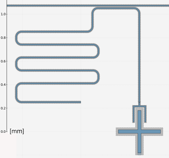
Figure 1: Design rendered in Qiskit-Metal GUI. (a) Zoom on the Xmon qubit: this type of qubit consists of a Josephson Junction shunted by a cross-shaped capacitance. (b) Xmon qubit capacitively coupled to a quarter wave resonator for readout. The readout resonator is also capacitively coupled to the feedline.
Circuit Simulation and Parameter Extraction
Simulations are performed using Ansys Q3D and Ansys HFSS to extract critical capacitance values and perform eigenmode analysis. The Q3D results yield precise capacitance values necessary for accurate modeling, such as the qubit shunt capacitance (Cs) and the qubit-resonator coupling capacitance (Cg). These parameters are foundational in deducing the system's resonant frequencies, anharmonicity, and qubit-resonator couplings. Ansys HFSS enables the Energy Participation Ratio (EPR) analysis for further refinement of the qubit parameters.
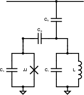
Figure 2: Lumped element circuit equivalent of our design. The resonator is represented as an LC circuit (Lr, Cr), while the qubit is a Josephson Junction shunted by a capacitance (Cs). Cg is the qubit-resonator coupling capacitance and Ck is the resonator-feedline coupling capacitance.
The qubit and resonator frequencies derived from simulation closely match expected values, with a detuning significant enough to facilitate effective qubit-resonator interaction. The coupling strength and the dispersive shift have been calculated, yielding $g_{01}/2\pi = \SI{47.38}{\mega\hertz}$ and $\chi/2\pi = \SI{-1.44}{\mega\hertz}$ respectively, indicative of a robust qubit-readout process. The relaxation time for the qubit (T1) is estimated at approximately $\SI{13}{\micro\second}$, aligning with theoretical expectations for such designs. Discrepancies between simulated and theoretical values are minor and can be attributed to modeling limitations and parameter variability in practical implementations.
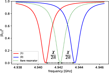
Figure 3: Feedline transmission as a function of frequency when the qubit is in the ground (blue) or excited state (red).
Conclusion and Future Directions
This paper successfully delineates the initial design and parameter extraction for a superconducting qubit intended for advanced quantum sensing applications. While the design and simulations are consistent with theoretical projections, ongoing efforts are aimed at optimizing the device for improved anharmonicity and relaxation times. Inductive coupling and parameter tuning of the qubit-Josephson junction system represent promising avenues for future enhancement. The transition from simulation to actual fabrication will serve as a critical phase in validating the design procedures outlined in this study. Further research will likely focus on refining design methodologies to achieve even greater operational efficacies.