Huawei's Chip Was Supposed to Melt?
Abstract: Heat is the sharpest concern on scaling law --- the time-scaling principle behind Huawei's folded silicon, named for the delay (``Tao'') it sets out to shrink. Our Kirin measurements turned that objection upside down. The reason is one every commuter already knows: on a chip, as in a workday, it is the travel that burns the majority of the energy, not the work at the desk.
Paper Prompts
Sign up for free to create and run prompts on this paper.
Top Community Prompts
Explain it Like I'm 14
1. What is the paper about?
This paper asks a surprising question: Why did Huawei’s densely stacked computer chip become cooler instead of hotter?
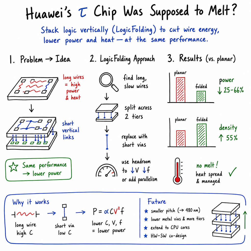
Normally, putting more transistors into a small space seems likely to create more heat. Huawei’s idea, called LogicFolding, stacks parts of a chip on top of each other using 3D technology. The paper argues that this can actually reduce power use because signals do not have to travel as far.
The main example is Huawei’s Kirin 2026 smartphone processor.
2. What questions does the paper try to answer?
The paper focuses on several main questions:
- Can a chip become more powerful without making its transistors smaller?
- Does stacking chip layers make overheating worse?
- Where does most of a chip’s energy go: doing calculations or moving data?
- Can shorter connections between parts of a chip reduce power use?
- Can a chip be both denser and cooler at the same time?
The authors argue that the answer to the last question is yes, if the chip is carefully designed.
3. How does LogicFolding work?
The basic idea
Traditional chips are mostly flat. Their components are spread across one layer, and signals travel sideways through long metal wires.
LogicFolding changes this by placing parts of a circuit on two or more layers, like floors in a building. Very small vertical connections join the layers.
An analogy is a city:
- In a flat chip, people may need to travel long distances across roads.
- In a folded chip, important buildings can be placed directly above one another.
- Elevators between floors replace long journeys across the city.
These vertical connections are made using a process called 3D hybrid bonding. Two thin pieces of silicon are carefully lined up and joined. Their metal connection points fuse together, creating many tiny paths between the layers.
Why shorter wires matter
Moving data through a chip uses energy. A long wire is like a long road: it takes more effort to send signals along it. A short wire is like a nearby road and requires less energy.
The paper describes power using this simplified relationship:
This means that power depends on:
- : how much electrical “capacity” the wires and circuits have,
- : voltage,
- : how quickly the circuit switches,
- : how often the circuit is active.
The most important point is that the wires can use more energy than the transistors doing the calculations. In the paper’s analogy, the transistors do the “desk work,” while the wires handle the “commute.” The commute can cost more energy than the work itself.
LogicFolding shortens this commute.
How the researchers tested it
The authors compared the folded Kirin 2026 with the earlier flat Kirin 9030 Pro. They examined important parts of the processor, including:
- The NPU, which performs artificial-intelligence calculations.
- The GPU, which creates images and video.
- The CPU, which handles general computer tasks.
- The DSP, which processes signals such as audio and communications data.

They measured performance, clock speed, voltage, power consumption, and power density. They often compared the chips while doing the same amount of work, such as producing the same number of images per second or completing the same AI task.
This is called an iso-performance comparison. It is like comparing two cars while asking both to travel at the same speed. The question is then: which car uses less fuel?
4. What did the paper find?
More transistors in the same space
The Kirin 2026 reportedly increased transistor density from about 155 million to 238 million transistors per square millimeter.
That is a 55% increase in the number of transistors packed into the same area.
Major power savings
Despite having more transistors, the chip used less power when performing the same tasks:
| Chip section | Reported power reduction |
|---|---|
| NPU | 66% |
| GPU | 58% |
| CPU performance core | 41% |
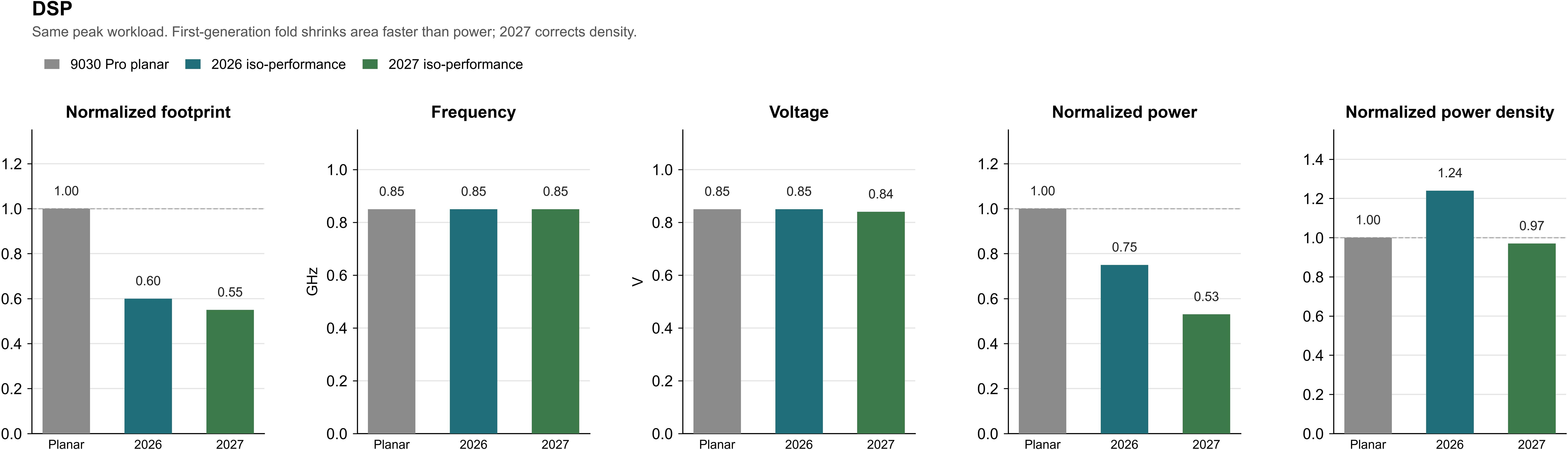
| DSP, first folded version | 25% |
The NPU showed especially large improvements. At the same performance level, its clock speed could be reduced by 63%, and its voltage could drop from 0.85 volts to 0.55 volts. As a result, its power density reportedly fell by 73%.
Shorter connections
The paper says LogicFolding shortened many signal paths by about 20%, and some important paths by as much as 70%.
The clock network also became much simpler. In one example, the number of clock buffers fell from 43,600 to 19,000. Clock buffers help distribute timing signals around a chip, so needing fewer of them can save energy.
More performance when needed
The folded chip was not only more efficient. When run at full power, it could also be faster:
- The NPU reached 70 trillion operations per second, or TOPS.
- The GPU produced up to 42% more frames.
- The CPU’s benchmark score increased by 18%.
This means the chip could be operated in two ways: as a cooler, more efficient chip or as a faster chip using more power.
Not every result was perfect
The DSP showed an important warning. In the first folded design, its total power use fell by 25%, but its power density increased by 24%. This happened because the DSP became much smaller, concentrating its remaining power into a smaller area.
The authors say that a later design fixed this problem. The newer version reportedly used 47% less power and had lower power density than the original flat design.
This shows that 3D stacking does not automatically solve every heating problem. Engineers must decide carefully where to place hot and cool parts.
5. Why can a denser chip be cooler?
The paper gives two main explanations.
First: shorter data journeys
A large amount of chip power is spent moving information through wires. By placing related circuits closer together, LogicFolding reduces the distance signals travel.
This lowers the wires’ electrical capacitance and reduces the energy needed to charge and discharge them.
Second: more parallel processing
The extra space created by stacking can be used to add more copies of certain circuits. Instead of one circuit working extremely hard and quickly, several circuits can share the work.
Each circuit can then operate at a lower speed and lower voltage.
This is especially useful because power depends on the square of voltage. For example, lowering voltage by a small amount can produce a much larger reduction in power.
The paper compares this idea with Amdahl’s law, which says that a computer program can only benefit from parallel processing when enough of its work can be split into separate tasks. The authors argue that most NPU, GPU, and DSP work can be split up, while some CPU tasks still need one fast processing path.
6. How did the researchers deal with heat?
The authors say that average chip temperature is not the only important issue. The most dangerous problem is a hotspot, where one small region becomes much hotter than the rest.
They tried to control this by:
- Reducing the total power used at the same performance.
- Spreading heat across multiple layers and across the chip.
- Placing hot and cool circuits carefully.
- Avoiding the direct stacking of several very hot areas.
- Designing the chip so heat has easier paths to escape.
The paper says the Kirin 2026 used a cautious version of LogicFolding. Huawei folded the paths that gained the most from shorter connections instead of stacking every part of the chip indiscriminately.
7. Why are the findings important?
The findings challenge the common belief that more transistors in a smaller space must always mean more heat.
The paper’s central lesson is:
A chip’s energy use depends not only on how many transistors it has, but also on how far signals must travel and how the work is divided.
This could be important because shrinking transistors has become increasingly difficult. If engineers cannot keep making transistors smaller, they may still improve chips by:
- Stacking silicon layers.
- Shortening connections.
- Adding more parallel processing units.
- Reducing voltage and clock speed when maximum performance is not needed.
- Designing hardware and software together.
These techniques could help future smartphones, AI processors, graphics chips, and data-center computers use less energy.
8. Overall conclusion
The paper argues that Huawei’s folded chip did not overheat because LogicFolding reduced the amount of energy spent moving data. The chip had more transistors, but many of its signals traveled much shorter distances. Its extra circuitry also allowed more tasks to run in parallel at lower voltage.
The results suggest that 3D chip stacking can sometimes improve both performance and energy efficiency, rather than automatically causing a heat crisis.
However, the paper also admits that this is not a magic solution. It is based largely on Huawei’s reported measurements, and careful thermal design is still necessary. Some parts of a processor benefit more than others, and future chips will need better bonding methods, more advanced design tools, and improved ways to remove heat.
In simple terms, the paper says: A crowded chip is not necessarily a hot chip. If its parts are placed intelligently, making the journey shorter can save more energy than the extra parts consume.
Knowledge Gaps
Knowledge gaps, limitations, and open questions
- Independent validation is absent: The reported Kirin 2026 and Kirin 2027 results are presented without independent measurements, third-party replication, or publicly available silicon, test boards, or raw datasets.
- Experimental methodology is underspecified: The paper does not report measurement equipment, workload duration, temperature conditions, power-sampling locations, statistical variation, confidence intervals, or the number of tested chips.
- The comparison with the Kirin9030 Pro is not fully controlled: It is unclear whether the predecessor and folded chip use comparable process technologies, memory systems, packaging, firmware, cooling solutions, transistor libraries, and operating conditions.
- The source of the reported power reductions is not quantitatively decomposed: The paper does not separate savings from shorter interconnects, lower voltage, reduced frequency, architectural changes, clock-tree redesign, software optimization, and process or packaging differences.
- The claim that wires dominate dynamic power is not demonstrated for the reported designs: No capacitance breakdown is provided for gate, local-interconnect, global-interconnect, clock-network, memory, and I/O components across the NPU, GPU, CPU, and DSP.
- The relationship between wire-length reduction and energy reduction remains unverified: Reported reductions of 20–70% in wire length are not linked to measured changes in capacitance, RC delay, switching activity, or energy per operation.
- Power-density definitions are incomplete: The analysis does not clearly define whether power density includes only active logic, interconnects, memory, bonding structures, leakage, regulators, or inactive regions, nor how the projected footprint of a two-tier stack should be compared with a planar footprint.
- Thermal evidence is insufficient: The paper asserts lower junction temperatures but does not provide measured junction-temperature maps, thermal resistance, thermal conductivity, transient thermal responses, or direct comparisons of top-tier and bottom-tier temperatures.
- Hotspot mitigation is not experimentally demonstrated: The proposed thermal-aware placement and interleaving of hot and cool logic are described conceptually, but no placement results, hotspot maps, or ablation studies show how much these techniques reduce peak temperature.
- Transient and sustained thermal behavior is unresolved: The measurements appear focused on benchmark operating points and do not establish whether the folded chip remains thermally stable during prolonged, bursty, or simultaneous CPU/GPU/NPU workloads.
- Reliability effects of elevated bottom-tier temperatures are unexplored: The paper does not evaluate electromigration, bias-temperature instability, time-dependent dielectric breakdown, thermal cycling, inter-tier stress, or lifetime degradation caused by vertical thermal gradients.
- Hybrid-bonding reliability is not characterized: The effects of voids, bond defects, contamination, misalignment, wafer bow, bonding stress, annealing, and mechanical warpage on long-term electrical performance and yield are not reported.
- Manufacturing yield and defect tolerance are missing: No data are provided on wafer-level bonding yield, known-good-die strategy, repairability, redundancy, binning, or the probability that defects in one tier invalidate the entire stack.
- The economic feasibility claim is unsupported: The paper does not quantify equipment costs, process-cycle time, wafer utilization, yield loss, bonding costs, testing costs, or cost per functional chip relative to advanced planar and conventional 3D alternatives.
- Scalability beyond two tiers is uncertain: The claimed benefits, thermal behavior, yield, alignment requirements, and power delivery challenges for three or more active tiers are not modeled or experimentally evaluated.
- Power delivery and signal-integrity constraints are underexplored: The paper does not analyze vertical power delivery, IR drop, ground bounce, crosstalk, simultaneous switching noise, electromagnetic interference, or signal integrity at the proposed bonding pitches.
- The feasibility of sub-micrometer bonding pitches remains speculative: The expected transition to 720 nm and 480 nm is presented as a roadmap, but no demonstrated alignment tolerance, defect rate, process window, or electrical characterization supports these projections.
- Lower-metal-layer bonding is not validated: The proposed integration of bonding pads with lower metal layers may introduce routing, parasitic, reliability, and process conflicts that are not examined.
- Clock-network improvements are not generalized: The reduction from 43,600 to 19,000 clock buffers is reported for one block, but the paper does not establish whether similar savings occur across different architectures, clock domains, or physical-design constraints.
- Performance benefits are benchmark-dependent: The reported gains rely on selected workloads, including a specific game frame and proprietary HNX slices, leaving general-purpose application performance, worst-case workloads, and workload variability unresolved.
- Benchmark representativeness is unclear: The paper does not explain how the selected workloads represent typical smartphone usage, nor whether the results hold for multitasking, background activity, thermal throttling, and application-level responsiveness.
- Software–hardware co-design benefits are not isolated: The contribution of schedulers, task partitioning, compiler changes, and software parallelization is not separated from the contribution of LogicFolding itself.
- The limits imposed by serial workloads remain unquantified: The paper invokes an Amdahl-like hardware analogy but does not measure the serial fraction of each block or identify workloads for which folding provides little or no benefit.
- Memory and data-movement bottlenecks are insufficiently addressed: The analysis focuses on intra-block wiring but does not quantify effects on cache, SRAM, DRAM, interconnect-to-memory traffic, memory bandwidth, and energy consumed outside the folded blocks.
- Static leakage and low-utilization behavior are not evaluated: The claim that leakage is minimal may not hold across process corners, elevated temperatures, standby modes, or always-on smartphone workloads.
- Voltage-scaling limits are not established: The paper does not report voltage-frequency curves, minimum operating voltages, error rates, timing margins, or process-voltage-temperature variation for the folded tiers.
- Area and transistor-density accounting is ambiguous: It is unclear whether the 55% density increase includes both tiers, excludes bonding and peripheral overhead, or compares equivalent functional capacity and SRAM content.
- The claimed “ scaling law” lacks formal validation: The paper does not define a general mathematical law, identify its scaling parameters, establish predictive equations, or demonstrate that the reported results distinguish scaling from conventional physical-design optimization.
- No ablation study tests LogicFolding independently: A planar design with equivalent architectural changes, clock optimization, voltage reduction, and transistor redistribution is not presented as a control condition.
- Generality across process nodes and manufacturers is unknown: The results are based on one Huawei design and one reported bonding process; applicability to other technologies, foundries, device types, and design ecosystems remains unestablished.
- EDA and verification complexity is not quantified: The paper identifies tool-chain and verification challenges but provides no data on design time, routing closure, timing closure, thermal simulation cost, formal verification, or post-silicon debug complexity.
- Inter-tier test and repair procedures are not described: The ability to probe, diagnose, test, and screen stacked active tiers—especially when one tier fails—is left unresolved.
- The long-term impact on battery life is not measured: Lower block power at selected iso-performance points is not translated into whole-device energy consumption, battery endurance, or user-level battery life under realistic usage patterns.
Practical Applications
Immediate Applications
- Thermally efficient smartphone SoCs — consumer electronics
- Apply selective LogicFolding to communication-intensive blocks such as NPUs, GPUs, DSPs, and cache/interconnect regions rather than stacking the entire chip.
- The reported results suggest that, at matched performance, this approach could reduce power in AI, graphics, and CPU blocks while maintaining or lowering junction temperature. Potential products include longer-battery-life smartphones, thinner devices, and phones that sustain performance for longer before thermal throttling.
- A practical workflow would combine hybrid-bonded chip tiers with thermal-aware floorplanning, hotspot avoidance, and dynamic voltage/frequency scaling.
- Dependencies: high-yield wafer-to-wafer hybrid bonding; sub-micrometer alignment; accurate thermal models; smartphone software capable of distributing workloads across efficient and performance cores. The reported Kirin results are manufacturer claims and require independent replication across workloads and devices.
- Lower-power on-device AI inference — AI hardware and edge computing
- Use the additional transistor budget created by vertical integration to implement more parallel NPU units, allowing inference to run at lower frequency and voltage.
- Potential tools and products include smartphone generative-AI accelerators, real-time translation, image enhancement, speech recognition, and privacy-preserving local inference with lower energy consumption.
- The paper’s reported NPU example—maintaining 29 TOPS at substantially lower voltage and power—supports a design strategy in which added hardware is used for parallelism rather than peak clock speed.
- Dependencies: algorithms must expose sufficient parallelism; memory bandwidth and data movement must not become the new bottleneck; compiler and runtime support is needed to map workloads efficiently onto the folded NPU.
- Energy-efficient mobile graphics — gaming and visualization
- Apply folding to GPU datapaths, shader interconnects, clock networks, and local buffers to shorten high-traffic routes.
- This could support longer sustained gaming sessions, lower device surface temperatures, and improved performance-per-watt in augmented-reality and computational-photography workloads.
- A product workflow could offer two operating modes: an efficient mode that spends LogicFolding’s timing headroom on lower voltage, and a turbo mode that spends it on higher frame rates.
- Dependencies: sustained thermal testing is necessary because peak performance may still increase power density, as the paper reports for turbo operation.
- Clock-network and interconnect optimization — semiconductor design
- Use the reported reduction in clock wiring and buffer count as a concrete design target for folded SoC blocks.
- EDA flows could identify long, high-capacitance routes and automatically propose vertical links, tier assignments, buffer removal, and clock-tree restructuring.
- This is applicable to CPUs, GPUs, NPUs, DSPs, networking chips, and other communication-intensive designs.
- Dependencies: current commercial EDA tools, timing signoff, power-integrity analysis, and thermal-aware placement must support 3D physical design; vertical links must provide lower total RC than the horizontal alternatives after fan-out and bonding overhead are included.
- System-technology co-optimization — semiconductor engineering practice
- Adopt the paper’s STCO approach as a design methodology: jointly optimize transistor allocation, circuit partitioning, hybrid-bonding pitch, voltage/frequency targets, workload scheduling, and thermal placement.
- Companies could create design-space-exploration tools that compare planar, chiplet, and folded implementations using metrics such as energy per operation, junction temperature, wire length, bonding yield, and manufacturing cost.
- This is immediately actionable for research teams and advanced product-development programs even before the most aggressive bonding pitches are available.
- Dependencies: accurate cross-layer models and close coordination among architecture, circuit, packaging, process, and software teams.
- Workload-aware power management — operating systems and mobile software
- Mobile schedulers can classify applications by serial and parallel fractions, dispatching parallelizable tasks to multiple efficient cores or accelerators while reserving performance cores for inherently serial work.
- Potential software features include battery-aware AI scheduling, thermal-budget APIs, and application-level controls that trade latency for energy.
- This directly operationalizes the paper’s analogy between Amdahl’s law in software and the “serial fraction” of hardware.
- Dependencies: application workloads must be sufficiently parallel; scheduling overhead, memory contention, and latency constraints must be modeled rather than assuming all tasks can be distributed freely.
- Thermal-aware chip floorplanning — product reliability and validation
- Use hotspot maps and junction-temperature estimates to avoid placing multiple high-activity blocks directly above one another.
- Thermal-aware placement can be integrated into design rules, verification checklists, and production test suites for 3D SoCs.
- It may improve reliability by reducing temperature-induced leakage, timing variation, electromigration, and long-term aging.
- Dependencies: models must capture vertical thermal gradients, package and enclosure effects, workload transients, and manufacturing variation. Average chip temperature alone is insufficient.
- Energy-performance benchmarking — academia and industry evaluation
- Evaluate folded designs at iso-performance, not only at maximum throughput. Useful metrics include energy per inference, energy per rendered frame, power density, junction temperature, sustained performance, and performance per watt.
- This would prevent misleading comparisons in which a folded chip appears efficient only because it runs slower, or appears inefficient only because it is tested in turbo mode.
- Dependencies: standardized workloads, independently reproducible measurements, and disclosure of footprint definitions—particularly for comparing projected two-tier area with planar area.
- Advanced semiconductor education and research
- The paper provides a practical case study for courses and laboratories covering interconnect-dominated power, , 3D integration, thermal design, Amdahl’s law, and STCO.
- Students and researchers can reproduce simplified experiments using floorplanning and circuit simulators to compare long horizontal wires with short vertical interconnects.
- Dependencies: access to realistic 3D EDA models and process parameters; simplified simulations should not be presented as substitutes for silicon measurements.
Long-Term Applications
- Multi-tier logic processors — high-performance computing and data centers
- Extend LogicFolding from two tiers to three or more active logic layers, using vertical integration to reduce communication distance within CPUs, GPUs, AI accelerators, and networking processors.
- Potential benefits include higher compute density, lower interconnect energy, and increased performance per rack or per unit of data-center floor space.
- The approach is especially relevant where data movement dominates computation, such as large AI models and graph-processing systems.
- Dependencies: heat removal from inner tiers, power delivery, yield stacking, repairability, cooling infrastructure, and economic scaling. Data-center workloads may also be limited by off-chip memory and network traffic rather than on-die wiring.
- 3D AI accelerators with vertically distributed memory — AI and data-center infrastructure
- Combine folded compute arrays with vertically adjacent SRAM, cache, or high-bandwidth memory to reduce the energy cost of moving activations and weights.
- Possible products include inference accelerators for data centers, autonomous systems, scientific computing, and large-scale recommendation services.
- The paper’s central finding—that communication can dominate computation—supports prioritizing memory and interconnect placement alongside arithmetic density.
- Dependencies: memory thermal limits, bandwidth matching, error correction, fabrication compatibility, and software support for nonuniform three-dimensional memory hierarchies.
- Energy-efficient edge devices and embedded systems — robotics, automotive, and IoT
- Deploy folded NPUs, DSPs, and sensor-processing blocks in robots, drones, cameras, industrial controllers, and vehicles.
- Lower power per operation could enable longer battery life, passive or compact cooling, and more local processing with reduced reliance on cloud services.
- Example workflows include local object detection, sensor fusion, predictive maintenance, navigation, and machine-vision inspection.
- Dependencies: automotive and industrial qualification, operation across wide temperature ranges, long product lifetimes, functional safety, and resistance to vibration and manufacturing defects.
- High-performance mobile CPUs — future smartphone and laptop processors
- Apply more advanced folding to relatively serial CPU cores, where the paper acknowledges that benefits are smaller and design complexity is higher.
- If successful, future processors could achieve higher frequencies or equivalent performance at lower voltage by shortening critical paths and selectively duplicating or parallelizing portions of the core.
- Potential products include fanless laptops, high-performance tablets, and mobile workstations.
- Dependencies: substantial EDA innovation, long verification cycles, branch-heavy workload behavior, cache latency, software compatibility, and the limited parallelizability described by Amdahl’s law.
- Standardized hybrid-bonding manufacturing platforms — semiconductor fabrication and packaging
- Develop broadly available wafer-to-wafer and die-to-wafer processes with bonding pitches approaching top-metal pitches, together with known-good-die strategies and automated alignment.
- Such platforms could enable folded logic, 3D cache, sensor-processor integration, and heterogeneous chip stacks across multiple foundries.
- Potential commercial tools include bonding-yield monitors, wafer-bow correction systems, thermal-stress inspection, and 3D interconnect design kits.
- Dependencies: defect propagation between bonded wafers, thermal expansion mismatch, CMP and surface cleanliness, bonding yield, test access, supply-chain investment, and standards for inter-die interfaces.
- 3D EDA and automated folding tools — software industry
- Create synthesis and physical-design systems that automatically partition a 2D circuit into tiers according to timing, wire capacitance, voltage domains, thermal constraints, and bonding availability.
- These tools could generate alternative designs optimized for energy, frequency, area, or reliability and estimate the break-even point at which vertical links outperform horizontal routing.
- Dependencies: accurate parasitic extraction for hybrid bonds, multi-tier timing analysis, thermal-electrical co-simulation, manufacturability rules, and integration with existing verification flows.
- Adaptive workload placement based on thermal geography — operating systems and robotics
- Future systems could monitor per-tier temperature and activity, then migrate tasks to avoid persistent hotspots or exploit cooler regions of the stack.
- In robots, vehicles, and mobile devices, thermal-aware scheduling could dynamically select between local accelerators, CPU cores, and cloud offload.
- Dependencies: fine-grained temperature sensors, low-overhead task migration, predictable real-time behavior, and software models that account for thermal transients rather than only average power.
- Energy-aware policy and procurement standards — government and industry regulation
- Policymakers and large technology purchasers could encourage reporting of energy per task, sustained performance, power density, and junction temperature for advanced processors.
- Standards could require separate disclosure of iso-performance and peak-performance results, reducing incentives to optimize only for short benchmark bursts.
- Public procurement programs could favor processors that deliver specified AI, graphics, or sensing workloads within thermal and energy budgets.
- Dependencies: internationally consistent benchmarks, independent verification, protection against selective workload reporting, and lifecycle accounting that includes the energy and materials required to manufacture complex 3D stacks.
- Battery and thermal-management improvements in daily-life electronics
- If the reported power reductions generalize, phones, wearables, cameras, and portable medical devices could operate longer between charges and require less aggressive cooling.
- Products might use smaller batteries for the same operating time, or retain current battery capacity while adding more local AI and sensing functions.
- Dependencies: real-world application mix, display and radio power—which may dominate total device consumption—battery aging, software behavior, and whether the chip’s extra capability causes users or applications to demand more computation.
- Research into the limits of time-based scaling
- Academic work could test whether the proposed scaling framework generalizes beyond the reported mobile SoC to chiplets, photonic interconnects, neuromorphic systems, and quantum-control electronics.
- Key research questions include whether reduced wire delay consistently produces lower energy, how benefits scale with tier count, and when bonding, cooling, or serial computation becomes the limiting factor.
- Dependencies: independent silicon evidence, transparent experimental methods, comparisons with advanced planar and chiplet baselines, and careful separation of improvements caused by LogicFolding from those caused by voltage scaling, architectural redesign, or software scheduling.
Glossary
- Amdahl’s law: Principle stating that a program’s serial portion limits the speedup achievable through parallelism. “Amdahl's law is about software.”
- Anneal: To heat a material under controlled conditions to alter or strengthen its structure. “During the anneal, covalent bonds form across the two oxide surfaces”
- Clock buffer: A circuit that distributes and maintains the timing signal across a chip. “we cut clock-buffer count by more than half.”
- Clock frequency: The rate at which a processor’s clock cycles, usually measured in hertz. “its clock frequency could be dialed down by 63\%”
- CMP planarization: Chemical mechanical polishing used to create a flat semiconductor surface. “stress control, CMP planarization, cleaning, wafer bow, edge taper, and alignment”
- Critical path: The longest or most timing-sensitive sequence of operations that determines a circuit’s maximum speed. “the characteristic delay a signal takes to travel a chip's critical paths.”
- Die: An individual piece of semiconductor material containing an integrated circuit. “Two wafers --- or a wafer and a chip --- are carefully aligned”
- Die-to-wafer bonding: A process that attaches individual semiconductor dies to a complete wafer. “Die-to-wafer bonding is a die-handling process --- pick and place”
- Dynamic energy: Energy consumed when circuit signals switch between logic states. “Digital circuits essentially consume dynamic energy in two ways.”
- Dynamic power: Power consumed by switching activity in a digital circuit. “Its opposite, dynamic power, what's lost during computing, makes up roughly 90\% of the total power bill.”
- EDA toolchain: A collection of electronic design automation tools used to design, simulate, and verify integrated circuits. “Applying LogicFolding to low-parallelism CPU performance core requires meticulous design, advanced EDA toolchains, and long verification cycles.”
- EUV lithography: Extreme ultraviolet photolithography used to pattern extremely small features on semiconductor wafers. “Shrinking past what the industry calls the 7-nanometer node requires extreme ultraviolet (EUV) lithography”
- Fan out: To distribute a signal from a dense connection region to a wider or more widely spaced set of connections. “those signals must fan out to sparser pads”
- Geometric scaling: Increasing semiconductor performance by reducing the physical dimensions of transistors and related structures. “it has always leaned on a single trick: geometric scaling.”
- Hybrid bonding: A wafer- or die-joining technique that forms simultaneous dielectric and metal connections between semiconductor layers. “The enabling craft is called 3D hybrid bonding”
- Integrated circuit: An electronic circuit containing many interconnected components fabricated on a single semiconductor substrate. “Yet semiconductor progress is still told as a story about better transistors”
- Interconnect capacitance: Capacitance associated with the wires connecting circuit components. “Interconnect capacitance, not gate capacitance, is where the energy goes.”
- Iso-performance: A comparison condition in which different systems perform the same amount of work or achieve the same benchmark result. “we measured it by running the folded chip against its planar predecessor, the Kirin9030 Pro, at iso-performance”
- Junction temperature: The temperature at the semiconductor junctions where a transistor’s active electrical behavior occurs. “the junction temperature of transistors, which is the metric that actually governs speed, leakage, and reliability.”
- LogicFolding: The vertical restructuring of a circuit into stacked tiers to shorten signal paths and reduce delay or energy. “Its flagship technique for compressing that delay is called LogicFolding”
- Metal pitch: The center-to-center spacing between adjacent metal lines or connection features in an integrated circuit. “A typical logic process has a top-metal pitch of 720~nm.”
- NPU: A neural processing unit specialized for accelerating artificial-intelligence and machine-learning computations. “The NPU is the block critics most fear stacking because it is both the densest and among the hottest.”
- Overlay: The positional alignment accuracy between patterns formed in successive semiconductor-processing layers. “lithography tools already hold overlay to few nanometers.”
- Parallelism: The simultaneous execution of multiple computations or operations. “The serial work requiring high voltage is small enough not to dominate the power budget; everything else --- the vast parallel majority --- is folded wider”
- Power density: The amount of power dissipated per unit area or volume. “power density --- what's consumed per square millimeter”
- RC: The resistance-capacitance effects that contribute to signal delay and energy consumption in interconnects. “the resistance and capacitance that slow and tax every signal.”
- Serial fraction: The portion of a computation that cannot be parallelized and must execute sequentially. “a program's serial fraction limits how much parallelism can buy you.”
- SoC: A system-on-chip integrating processing, memory interfaces, and other computing functions into one semiconductor device. “On Kirin 2026, the first mobile system-on-chip (SoC) relying on LogicFolding”
- Static leakage: Power consumed by a circuit even when it is not actively switching. “One, static leakage, or the power lost even when no computing is happening, is minimal.”
- System-Technology Co-Optimization (STCO): A design methodology that jointly optimizes system architecture and semiconductor technology. “forming the theoretical bedrock of System-Technology Co-Optimization (STCO).”
- Thermal gradient: A spatial change in temperature across a material or device. “The modest vertical temperature gradient where the bottom tier runs a few degrees warmer than the top”
- Thermal-aware placement: Positioning circuit blocks to control heat distribution and avoid excessive local temperatures. “with thermal-aware placement rather than blindly stacking everything.”
- TSV: A through-silicon via, or vertical conductive connection passing through a semiconductor die. “integrating lower-metal TSVs”
- Wafer-to-wafer bonding: A process that joins two complete semiconductor wafers to form a multilayer structure. “Wafer-to-wafer bonding starts from a different world”
- Wafer bow: Curvature or warping of a semiconductor wafer caused by stress or processing conditions. “stress control, CMP planarization, cleaning, wafer bow, edge taper, and alignment”
- Wafer-level processing: Manufacturing or bonding operations performed while semiconductor devices remain arranged on a complete wafer. “We treat the hybrid bonding as a wafer-level, cross-layer device step rather than a packaging step.”

