- The paper introduces an in situ gold nanodisk calibration protocol that reduces systematic localization errors from 20–30 nm to below 1 nm using a Zernike polynomial model.
- It achieves sub-10 nm precision in quantum emitter localization, validated by improved polarization metrics and repeatable measurements.
- The method enhances deterministic integration of quantum dots into nanostructures, paving the way for scalable quantum photonic circuits.
Calibration of Systematic Distortions in Quantum Emitter Localization Microscopy for Nanophotonic Fabrication
Introduction
Accurate localization of quantum emitters and their deterministic integration into nanophotonic structures is central for scalable quantum photonic technologies, where single-photon sources such as self-assembled semiconductor quantum dots (QDs) play a foundational role. Although photoluminescence (PL) imaging combined with statistical analysis allows sub-10 nm precision in emitter localization, systematic distortions arising in custom microscopy setups lead to position-dependent biases that limit the true metrological accuracy achievable during subsequent nanofabrication steps. These distortions originate from nonideal optical elements, alignment imperfections, and aberrations in cryogenic microscopes, and can greatly exceed the inherent localization noise floor. This work presents an in situ, reference-based calibration protocol using lithographically fabricated gold nanodisk arrays, which enables the extraction and correction of spatially varying distortions using a Zernike polynomial vector field model.
The optical positioning approach is implemented on cryogenically cooled samples containing QDs grown by droplet etching and nanohole infilling in GaAs, which are then overlaid with fine-pitched gold nanodisk calibration arrays and alignment markers by electron beam lithography (EBL). The wide-field PL microscope operates with a bichromatic illumination scheme, registering both QD emission (excited at 450 nm) and marker/nanodisk reflection (illuminated at 810 nm) within a unified optical coordinate system. The optical axis is engineered to minimize geometric aberrations and mechanical vibration is characterized to assess system stability.
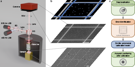
Figure 1: Schematic illustrating the wide-field PL microscope setup, nanodisk calibration array, and overall distortion calibration workflow.
The fundamental localization precision, extracted by 2D Gaussian fitting of QD PL spots and nanodisk reflection profiles, achieves a mean fitting uncertainty of 6.6 nm, with localization repeatability of 3.9 ± 6.2 nm under extended acquisitions. These metrics represent the lower bound set by optical and mechanical noise in the measurement system and are sufficient for stringent nanophotonic fabrication requirements.
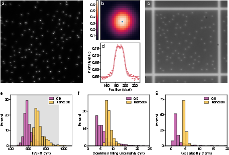
Figure 2: Performance characterization of optical positioning—PL and reflection images, fit statistics, and repeatability distributions for QD and nanodisk localizations.
However, systematic position-dependent offsets—measured as discrepancies between detected nanodisk positions and their lithographic design coordinates—dominate the overall localization error. These distortions, in the absence of correction, are on the order of 20–30 nm (mean) across the field of view, vastly exceeding stochastic fitting noise.
Distortion Modeling and Calibration Protocol
To achieve systematic calibration, the residual offset field is mapped via reference measurements of the gold nanodisk arrays distributed over the field of view. The observed distortion pattern, largely exhibiting a spatially varying pincushion component, is modeled as a vector field expressed as a weighted sum of Zernike polynomials up to Noll index n=10. This physically interpretable basis captures both low- and higher-order aberrations.
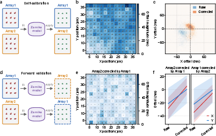
Figure 3: Self-calibration, offset mapping, model fitting, and forward validation of the Zernike-based optical distortion model on nanodisk reference arrays.
The optimal calibration parameters are identified by minimizing the L2-norm of corrected-detected-to-design coordinate residuals. Following calibration, mean systematic errors reduce to <1 nm, and the 2D scatter (standard deviation of residuals) is suppressed to 24.6 nm field-wide. These figures approach the combined stochastic and EBL overlay error limits.
The protocol’s predictive accuracy is rigorously benchmarked using a held-out array validation scheme: the Zernike model trained on one array is applied to another, yielding a corrected mean-offset of 5.3 nm and statistically comparable dispersions in both coordinate axes.
Application to Deterministic Nanophotonic Fabrication
The efficacy of distortion calibration in practical device fabrication is demonstrated by integrating localized QDs into circular mesa structures. Mesas are defined via EBL and dry etching, using both raw and distortion-corrected QD positions as inputs. Polarization-resolved micro-PL of the resulting devices provides a highly sensitive probe of emitter-mesa registration accuracy, as asymmetries in the mesa geometry or QD placement lead to characteristic polarization anisotropy in the emission.
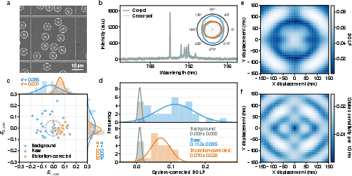
Figure 4: Polarization-resolved validation of registration accuracy: SEM of fabricated mesas, PL spectra, Stokes vector distribution, DOLP histograms, and simulated polarization sensitivity vs. displacement.
Strong numerical results are obtained: the mean device-to-device corrected DOLP (degree of linear polarization) decreases by 38%, and the standard deviation is reduced by 49% upon distortion correction. Monte Carlo simulations and FDTD modeling further corroborate that the residual anisotropy is dominated by minor mesa ellipticity, rather than misregistration, implying near-ideal QD centering on average. These metrics directly validate the impact of systematic distortion calibration for enhanced deterministic integration yield and device uniformity.
Implications and Future Directions
This work delineates the critical distinction between statistical localization precision and absolute registration accuracy in quantum emitter integration. The introduced nanodisk-based calibration, anchored by Zernike polynomial modeling, is broadly compatible with a wide array of emitters, imaging modalities, and nanofabrication workflows. The methodology offers significant practical benefit for scaling up deterministic quantum photonic circuit manufacturing, where placement fidelity is central for device arrays, multi-emitter systems, and hybrid photonic integration (2607.05370).
In the near term, this protocol could be generalized to alternative emitter types such as color centers and 2D material defects, and further refined through denser calibration arrays or advanced aberration correction algorithms. Future work may also combine this approach with machine vision calibration schemes, in situ SEM or cathodoluminescence mapping, or actively adaptive correction during fabrication runs. As system integration density increases and quantum photonic circuits become substantially larger and more complex, traceable, real-time calibration of localization distortions will be indispensable for maintaining yield and device performance.
Conclusion
A comprehensive reference-based calibration approach for systematic optical distortions is demonstrated, bridging the precision-accuracy gap that limits the yield in deterministic quantum emitter placement. Rigorous validation, both on reference arrays and functional device metrics, highlights the essential role of in situ calibration for reliable, scalable quantum photonic fabrication. The results firmly establish a route toward sub-10 nm metrological accuracy in wide-field localization microscopy, facilitating the next generation of integrated quantum technologies.