- The paper demonstrates that surface engineering in g-wave altermagnets converts bulk rank-5 multipoles into surface d-wave spin splitting, yielding a robust linear spin-splitter effect.
- The authors use a minimal tight-binding model and Kubo formalism to quantify charge-to-spin conversion, achieving a maximum SSE angle of 15°.
- The study reveals that weak surface ferromagnetism enables domain control, offering practical routes for spintronics device engineering.
Surface Functionalization of g-Wave Altermagnets: Enabling Spin-Splitter Effect via Thin Films
Introduction and Motivation
The paper "Functionalization of g-wave altermagnets: spin-splitter effect enabled by surfaces" (2607.04970) addresses the absence of linear spin-splitter effect (SSE) in bulk g-wave altermagnets, a notable challenge facing the exploitation of altermagnetic materials for efficient spin current generation in spintronics. This work rigorously demonstrates that surface engineering—specifically, the construction of thin-film or slab geometries—can induce a surface d-wave altermagnetism in otherwise bulk g-wave compounds, thereby unlocking substantial SSE functionality previously restricted to nonlinear regimes. The study utilizes a minimal tight-binding model and Kubo formalism to quantify the spin conductivity and conversion angle, exposing a robust bulk-boundary correspondence governed by magnetic multipolar order parameters.
The authors construct a minimal single-orbital tight-binding model motivated by the lattice structure of metallic g-wave altermagnets such as CrSb and MnTe. The bulk Hamiltonian features g-wave spin splitting proportional to a rank-5 magnetic multipole with characteristic momentum-dependence, F(k)=kykz(3kx2−ky2), resulting in complex spin textures and nodal planes.
Upon transitioning to slab geometry—with (210) surface orientation—the reduced symmetry at the surface enables the projection of the bulk g-wave order parameter onto a lower rank magnetic multipole, stabilizing g0-wave spin splitting at the boundary. This correspondence mirrors established principles in multipolar and topological physics, whereby bulk multipole moments induce boundary moments of lower rank.
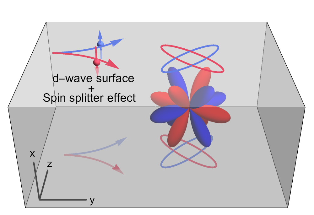
Figure 1: Schematic of a g1-wave altermagnet slab supporting surface g2-wave spin splitting, thereby enabling charge-to-spin conversion absent in the bulk.
Surface-Induced g3-Wave Altermagnetism and Spin-Splitter Effect
Diagonalization of the slab Hamiltonian at vanishing SOC demonstrates strong surface g4-wave spin polarization, with sign changes upon g5 rotation in reciprocal space and spin-degenerate axes coinciding with high-symmetry directions. Notably, both slab surfaces exhibit identical g6-wave spin patterns, leading to additive SSE contributions from each boundary.
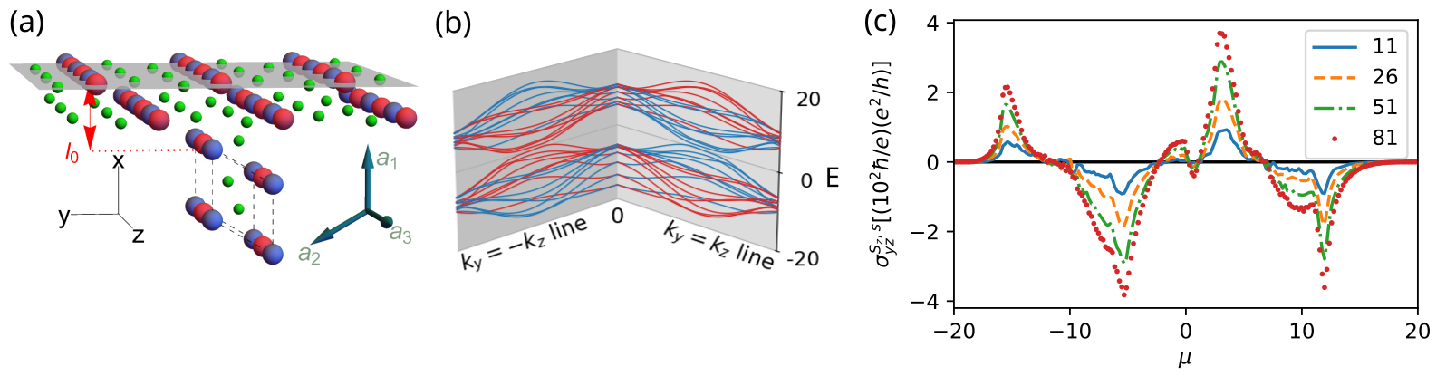
Figure 2: Panel (a) crystal structure of g7-oriented slab; (b) surface electronic band structure, highlighting g8-wave spin splitting; (c) spin conductivity g9 versus chemical potential for increasing slab thickness.
Applying the Kubo formula, the authors compute the off-diagonal spin conductivity g0, quantifying the transverse spin current generated upon application of a longitudinal electric field. The SSE is absent in bulk g1-wave altermagnets and only emerges due to the surface-induced g2-wave character. The results show that g3 increases with slab thickness, but the ratio to charge conductivity (defining the conversion angle) reveals the true efficiency. The maximum SSE angle achieved reaches g4, which is significant—comparable to values reported for strain-induced transitions to g5-wave order in CrSb.
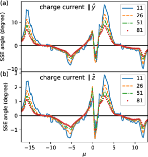
Figure 3: SSE angle as a function of chemical potential g6 for slabs of increasing thickness, measuring charge-to-spin conversion efficiency in principal axes.
The thickness dependence highlights the surface origin of the response: while total spin conductivity increases with thickness, charge conductivity increases faster, thereby diminishing efficiency for thicker slabs. Optimal conversion is achieved in the thinnest films, pointing towards practical thin-film engineering as a route to maximize SSE in non-g7-wave materials.
Weak Surface Ferromagnetism and Domain Control
A key finding is the emergence of weak surface ferromagnetism concomitant with the surface g8-wave altermagnetism. This weak magnetization, localized primarily at the surface layers and orders of magnitude below bulk moments, arises from symmetry reduction and finite relativistic effects. Importantly, this surface ferromagnetism enables linear Zeeman coupling to external fields, a mechanism unavailable for pure bulk g9-wave multipolar order (which couples only at fifth order). This paves the way for domain manipulation and field-induced enhancement of SSE by aligning altermagnetic monodomains.
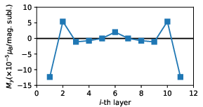
Figure 4: Layer-resolved d0-component of spin magnetization, highlighting the surface-dominated weak ferromagnetism in slabs of thickness d1.
Implications and Future Directions
The establishment of a bulk-boundary correspondence, wherein bulk rank-5 magnetic multipoles induce surface rank-3 moments and d2-wave altermagnetic states, has significant implications for material functionalization. The ability to engineer devices with tunable SSE via surface orientation, slab thickness, and external field manipulation expands the functional material landscape for spintronics beyond traditional d3-wave compounds.
Thin d4-wave AM films (e.g., CrSb) with appropriately chosen surface normal are now viable candidates for efficient charge-to-spin conversion, circumventing the need for large SOC or exotic strain application. The theoretical framework predicts that SSE optimization requires control over altermagnetic domains and thin-film fabrication techniques, both attainable with modern epitaxial growth and magnetometry.
Experimental verification, including detection of surface d5-wave splitting and weak magnetism at d6 scale, constitutes a direct path forward, integrating theoretical advances with practical materials realization.
Conclusion
This work demonstrates, via analytical modeling and Kubo formalism, that surfaces of d7-wave altermagnets can be functionalized to support robust d8-wave altermagnetism and substantial spin-splitter effect. The surface response exhibits strong charge-to-spin conversion efficiencies—up to d9 SSE angle—and is accompanied by weak surface ferromagnetism enabling domain control. The theoretical results strongly motivate thin-film engineering as a new platform for functionalizing non-g0-wave AMs for spintronic applications and underline the relevance of multipolar bulk-boundary correspondence in designing new functional materials.