- The paper introduces a novel digital accelerator for convolutional spiking neural networks that achieves 0.375 pJ/SOP energy efficiency by leveraging full kernel-level parallelism.
- It employs a unified memory system and event-driven convolution to minimize redundant state updates and optimize spike processing on a 22nm FDSOI platform.
- Experimental results on the DVS Gestures benchmark demonstrate 96.1% accuracy with scalable throughput, outperforming prior state-of-the-art accelerators.
Mega: A Digital Accelerator for Convolutional Spiking Neural Networks with State-of-the-Art Energy Efficiency
Introduction and Motivation
Mega presents a digital architecture for accelerating convolutional spiking neural networks (SNNs) on edge vision tasks, fabricated in GlobalFoundries 22 nm FDSOI technology. The design is motivated by the need to address three systemic challenges in convolutional SNN deployment: underutilization of convolutional parallelism (particularly for 3×3 kernels typical of SNN architectures), inflexibility in memory organization amid highly variable layer-wise demands, and inefficiencies in spike processing as input sparsity varies. Mega systematically targets these bottlenecks through architectural innovations that unlock both performance and energy advantages.
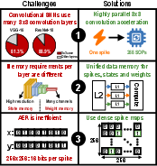
Figure 1: Challenges in accelerating convolutional SNNs (left) and Mega's architectural solutions (right), including parallel kernel processing, unified memory, and efficient spike handling.
Architecture and System Design
Mega centers its compute on nine highly parallel clusters, each responsible for one of the 3×3 convolution kernel offsets, collectively achieving full kernel-level parallelism. Each cluster integrates 32 convolution units (CUs), supporting 32 simultaneous output channel updates, thereby yielding 288 parallel neuron state operations per cycle. The design interlaces neuron state memory across nine dual-ported SRAM banks, a configuration devised to facilitate the concurrent access of a 3×3 window of neuron states and maximize bandwidth efficiency for highly parallel executions.
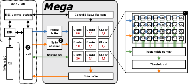
Figure 2: Core architecture with nine compute clusters, each handling 3×3 convolution in parallel across 32 output channels, interfacing with unified memory via the SNAX framework.
Mega introduces a unified memory for spikes, neuron states, and weights. This flexible memory subsystem, built on a TCDM with 32 SRAM banks, allows efficient data allocation strategies adaptable to disparate layer characteristics (e.g., large neuron states for initial layers vs. large weight storage for deeper layers). The RISC-V-based SNAX framework orchestrates configuration and data movement, offering a programmable control layer without penalizing cycle-level critical paths.
A spike streamer module dynamically converts dense binary spike maps into sparse representations using a pair of LZC (Leading Zero Counter) trees and lightweight address computation with LUTs, thereby minimizing overhead and stalling even at moderate sparsity levels.
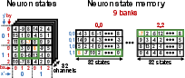
Figure 3: Neuron state memory is distributed across nine SRAM banks, enabling full-parallel window access and high-throughput channel processing.
Event-Driven Convolution and Pipelining
Mega implements event-driven convolution in lieu of the conventional frame-based approach, as computation in SNNs is fundamentally sparse and event-triggered. Upon an input spike, the architecture computes updates only for the relevant 3×3 neighborhood, reducing redundant state fetches and writes. The pipeline design in each convolution unit enforces address calculation, fetch, update with overflow handling, and write-back, with full RAW (Read-After-Write) hazard mitigation via address-based forwarding.
For thresholding and leak operations, each cluster includes a threshold unit capable of batch-processing neuron states, applying LIF (Leaky Integrate-and-Fire) function in a pipelined, row-wise manner. This design ensures spikes emitted by neurons are efficiently captured and transported without introducing cycle stalls or memory bottlenecks.
Silicon Implementation and Experimental Analysis
Mega occupies 1.12 mm² (23% of total SoC area) and operates in a voltage-frequency range from 0.55 V at 155 MHz up to 1.1 V at 600 MHz. Energy efficiency peaks at 0.375 pJ/SOP at minimum voltage, with sustained throughput of 38.4 GSOP/s, and scales up to 148.7 GSOP/s at higher performance points. Mega stands out for achieving these results without resorting to Compute-In-Memory (CIM) techniques, contrasting most recent state-of-the-art neuromorphic accelerators.
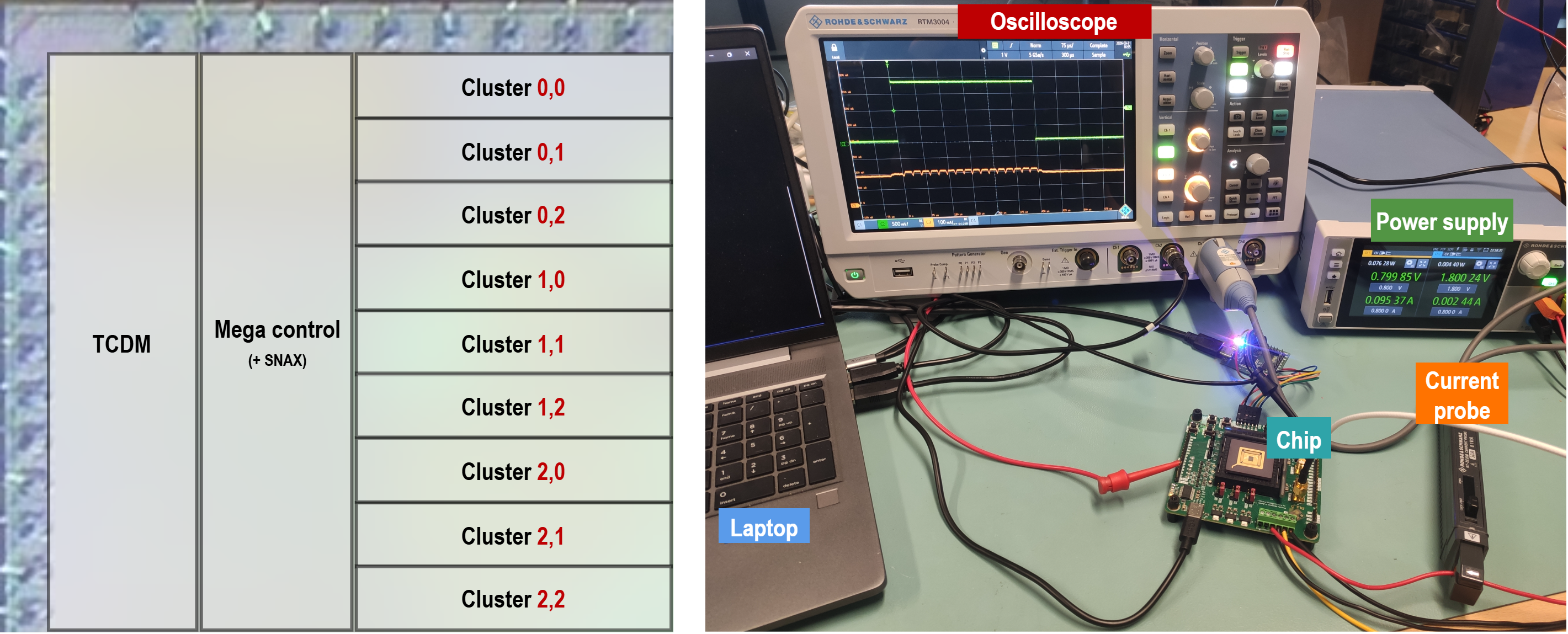
Figure 4: Chip micrograph and board-level measurement setup for direct silicon evaluation.
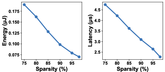
Figure 5: Measurement showing both energy consumption and inference latency scale favorably with increasing input map sparsity, validating event-driven efficiencies.
Energy and latency scale quasi-linearly with respect to input spike map sparsity, underscoring the benefit of event-driven convolution. Mega’s per-inference energy is 174.9 μJ on the IBM DVS gesture recognition task, and it delivers a strong accuracy of 96.1%, the highest reported for this benchmark in the evaluated hardware cohort.
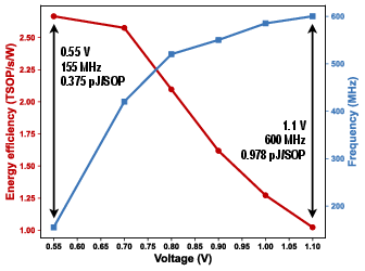
Figure 6: Voltage scaling plot demonstrates the tradeoff and flexibility between energy efficiency and throughput.
Application to SNN Vision Benchmarks
Mega was evaluated using a convolutional SNN (Figure 7) trained on the DVS Gestures dataset. The test harness measures both layerwise and aggregate throughput, energy, and accuracy, establishing quantitative superiority in both hardware metrics and real-world recognition rates.
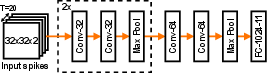
Figure 7: Multi-layer convolutional SNN network topology used for DVS gesture recognition benchmarking.
Comparison with Existing Accelerators
Comparison with neuromorphic accelerators such as RekOn, ANP-I, Sparse-IMC, SpiDR, and SpikeRAM demonstrates Mega's advantage in energy efficiency (0.375 pJ/SOP, a 4× improvement over the closest prior work), accuracy on DVS gestures (96.1%), and architectural flexibility for various SNN topologies. Importantly, these achievements are realized without CIM or analog in-memory MACs, validating the efficacy of the high-parallelism, event-driven digital approach.
Implications and Future Directions
Mega’s design highlights a shift toward extreme parallelism and flexible memory architectures to unlock the full potential of event-driven, sparse SNN computation for edge AI. The demonstrated energy efficiency and high accuracy suggest practical feasibility for battery-constrained, always-on vision systems in robotics, wearables, and IoT. Architecturally, the integration with a programmable host via SNAX also enables scalable, multi-accelerator solutions in larger heterogeneous systems.
Future work may focus on further co-optimizing the SNN training pipeline to specifically target Mega’s parallel structure and quantization scheme (INT4 weights, INT8 states), as well as expanding to support larger, more diverse SNN models and online learning mechanisms. Exploration of stacked and multi-chiplet integration could also push throughput boundaries while maintaining the demonstrated energy profile.
Conclusion
Mega delivers a substantial advancement in the hardware acceleration of convolutional SNNs, achieving state-of-the-art energy efficiency of 0.375 pJ/SOP, competitive inference accuracy, and scalable throughput on a physically realized 22 nm platform. Its architectural innovations in high-parallelism compute, unified memory organization, and efficient spike processing point to viable pathways for future neuromorphic computing systems targeting edge AI applications.
Reference: "Mega: A 22 nm Convolutional Spiking Neural Network Accelerator Achieving 0.375 pJ/SOP for Efficient Edge Vision" (2606.30039)

