- The paper demonstrates a novel inverse-design framework that integrates Guided Mode Expansion with analytical loss modeling to achieve significant improvements in bandwidth, dispersion, and loss reduction.
- It systematically maps trade-offs in photonic crystal waveguides, revealing order-of-magnitude enhancements in slow-light performance critical for both quantum photonics and optical communications.
- The approach enables robust broadband Purcell enhancement and compact phase shifter designs, with over tenfold bandwidth improvement and up to a 4x reduction in disorder-induced losses compared to conventional methods.
Inverse Designed Photonic Crystal Waveguides for Pulsed Operation: Dispersion, Losses, and Controlled Light-Matter Interactions
Introduction and Motivation
Photonic crystal waveguides (PCWs) provide a highly tailorable platform for controlling optical propagation, with strong potential for both classical and quantum photonic applications. Their ability to support slow-light modes with high spatial confinement enables engineered enhancement of light-matter interactions, vital for nonlinear optics, sensing, and quantum information processing. However, conventional approaches to PCW design face significant obstacles: practical devices typically require large low-loss bandwidths with a flat group index, yet this regime is impeded by inherent trade-offs between bandwidth, group velocity dispersion, and disorder-induced losses, especially near the photonic band edge.
The paper introduces a scalable inverse-design framework leveraging the Guided Mode Expansion (GME) method and physics-based analytical loss modeling within a constrained gradient-based optimization, achieving order-of-magnitude improvements in both computational efficiency and device characteristics. The work systematically delineates the parameter space—bandwidth, group index, normalized delay-bandwidth product (NDBP), dispersion, and loss—mapping trade-offs that set the practical limits of state-of-the-art PCWs. These methods are demonstrated for two crucial applications: broadband Purcell enhancement for quantum emitters, and high-speed, compact phase shifters for optical communication in Mach-Zehnder modulators (MZMs).
Methodology: Inverse Design with Analytical Loss Modeling
The core methodology integrates GME for efficient mode solving with an analytic disorder-induced backscattering loss model, supporting rapid evaluation of performance metrics (group index, bandwidth, loss, dispersion) as explicit functions of geometric parameters. The PCW geometry is parameterized by the position and radius vectors of select holes adjacent to the waveguide core, enabling constrained optimization over a sufficiently rich design space while respecting fabrication limits.
The cost function is constructed to minimize the deviation of group index from a target value across a chosen bandwidth region in k-space, subject to constraints for:
- Normalized loss below a specified threshold,
- Band edge and frequency window positioning,
- Single-mode operation (no overlapping bands),
- Fabrication feasibility (minimum hole radius and inter-hole separations).
Gradient-based optimization is performed using the trust-region method, with automatic differentiation facilitating efficient navigation of the high-dimensional design landscape.
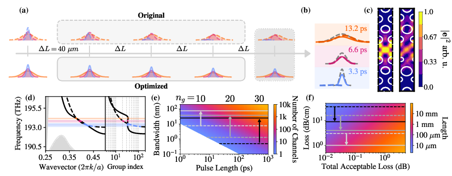
Figure 1: Inverse design yields large-bandwidth, slow-light PCWs with substantially improved bandwidth, loss, and pulse fidelity, as measured by pulse propagation profile, Bloch mode characteristics, and trade-off metrics compared to standard W1 designs.
Trade-Offs in Slow-Light PCW Optimization
A systematic exploration of the design space reveals emergent trade-offs between group index, normalized loss, NDBP, and dispersion. Calculations encompassing over 100 million mode calculations establish the boundaries of feasible device performance for telecom-band PCWs under realistic sidewall roughness.
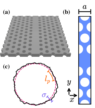
Figure 2: Left: 3D schematic and unit cell of PCW slab; right: representative fabrication roughness affecting disorder-induced loss.
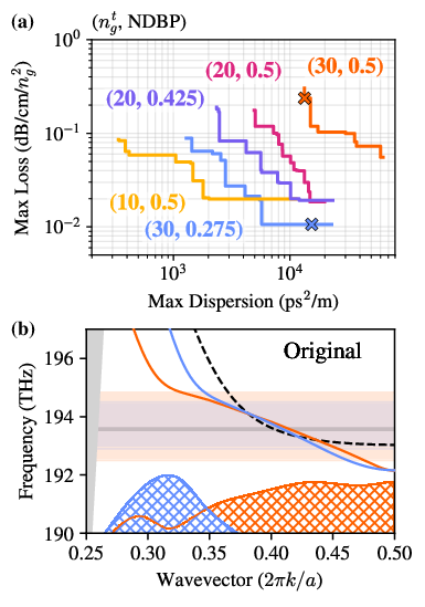
Figure 3: Large-scale optimization results show best-achievable combinations of loss and dispersion across a sweep of group index and normalized delay-bandwidth-product values, demonstrating the emergent Pareto fronts.
As the group index or bandwidth is increased, the design landscape contracts: it becomes more difficult to simultaneously engineer flat low-dispersion bands and maintain low loss, given the quadratic scaling of disorder-induced scattering with group index and the spatial overlap of slow-light Bloch modes with etched hole boundaries. Decreasing dispersion generally entails accepting higher loss, and vice versa; the optimal device lies along application-driven iso-loss or iso-dispersion contours in this space.
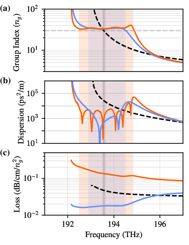
Figure 4: Optimized designs demonstrate significantly improved flatband group index (a), reduced and more uniform dispersion (b), and lower backscattering loss (c) compared to unoptimized W1 PCWs, within targeted spectral ranges.
Improvements of an order of magnitude in bandwidth and up to 4× reduction in loss are documented, directly translating to an increased number of information channels, greater device length tolerance, and improved pulse fidelity for ultrafast operation.
Broadband Quantum Photonics: Enhanced Purcell Factors
For on-chip quantum photonics, PCWs are employed to mediate efficient and broadband coupling between quantum emitters (e.g., InAs quantum dots, color centers in diamond/silicon) and propagating modes. The Purcell factor, scaling with group index and field localization at the emitter position, quantifies emission enhancement. Typical challenges include the inhomogeneous broadening of emitter ensembles and spatial randomness due to fabrication uncertainties.
The inverse design approach introduces explicit constraints to yield designs with both broad flat Purcell response—tolerant to frequency and position variation—and low propagation loss. For example, consistent Purcell factors above $5$ are demonstrated across ∼3.7 nm bandwidth, an order-of-magnitude improvement versus standard W1 PCWs, with only marginal sacrifice in propagation length.
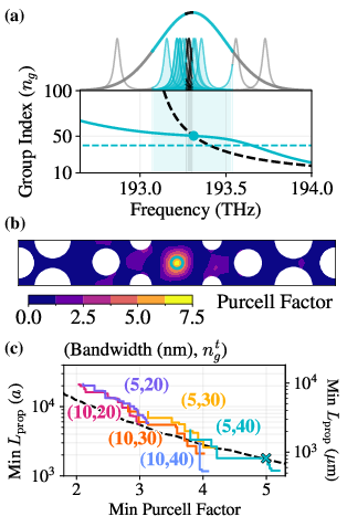
Figure 5: Optimized PCW for quantum emitter coupling achieves markedly increased flat group index (a), spatially uniform and enhanced Purcell factor (b), and favorable trade-off between loss length and minimum Purcell factor (c).
Such performance is crucial for scalable quantum photonic circuits, ensuring high indistinguishability and efficiency across spectral and spatially random ensembles of emitters.
Optical Communications: Compact, Broadband Phase Modulation
For integrated optical communications, PCW-based MZMs exploiting slow-light enhancements permit sub-millimeter phase shifters, essential for dense and fast photonic interconnects. The principal performance determinants include phase shift per unit length (Lπ), bandwidth, and total loss under practical doping and bias conditions.
Employing the analytic sensitivity of the PCW Bloch modes to local refractive index modulation in the doped slab, the framework supports phase-shift and loss-optimized design under constrained bandwidth and group index. Representative designs achieve over tenfold increase in bandwidth (from 1 nm to ∼15 nm) at fixed group index, with total device lengths as short as $0.26$ mm and losses as low as $1.9$ dB/cm, depending on the targeted trade-off between Lπ, bandwidth, and loss.
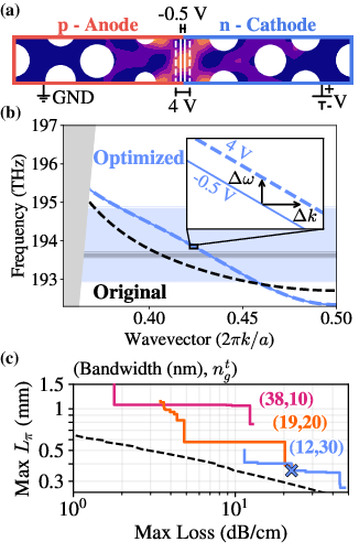
Figure 6: Optimized PCW MZM structure (a), increased flatband bandwidth and voltage-dependent phase sensitivity (b), and trade-off mapping between achievable device loss and phase shift length Lπ (c).
Such versatility enables bespoke device optimization for specific system requirements, balancing link budget constraints against footprint and energy efficiency.
Implications and Future Outlook
This work establishes a scalable, open-source pipeline for inverse-design of PCWs under concurrently optimized dispersion, loss, and application-specific figures of merit. The underlying use of GME and analytic perturbation models for loss and phase response enables exploration of large design spaces that are intractable with brute-force or black-box electromagnetic solvers, reducing computational cost by more than two orders of magnitude.
Implications include:
- Design of PCWs with ultra-broadband, flat, low-loss slow-light modes for multi-channel optical processing and communications.
- Customizable broadband quantum emitter-photon interfaces supporting scalable on-chip quantum networks.
- Application to other material platforms (e.g., GaAs, SiN) and modalities (e.g., topological photonics, non-reciprocal devices) given the open methodology.
- Compatibility with integrated nonlinear and electro-optic functionalities for all-optical and hybrid processing.
The documented parametric trade-offs establish design guidelines and theoretical limits, enabling rational application-specific PCW engineering. These advances serve as a foundation for the next generation of high-performance photonic circuits and quantum technologies.
Conclusion
The presented framework achieves simultaneous optimization of bandwidth, loss, and dispersion in PCWs through physics-informed, gradient-based inverse design. The resultant devices set new benchmarks for bandwidth and loss in both quantum photonics and integrated optical communication. The systematic mapping of the accessible parameter space, together with efficient, open-source computational tools, paves the way for more sophisticated and application-driven PCW technologies. The explicit trade-off curves and strong quantitative results will guide future experimental efforts and catalyze further developments in both the theoretical and applied domains of integrated nanophotonics.

