- The paper introduces a novel 4T differential FeFET bit-cell architecture that eliminates explicit backup cycles by enabling hybrid volatile and non-volatile memory modes.
- It leverages fully-depleted SOI FeFETs with an HZO ferroelectric layer, calibrated against experimental I-V data for robust differential sensing.
- Simulation and benchmarking reveal low write energy with 2 ns pulse widths and reduced cell area compared to conventional SRAM and nvSRAM designs.
A Novel FeFET Differential Bit-Cell With Hybrid Volatile and Non-Volatile Memory Modes
Introduction
The paper "A Novel FeFET Differential Bit-Cell With Hybrid Volatile and Non-Volatile Memory Modes" (2606.19918) introduces a 4-transistor (4T) differential memory bit-cell architecture that employs ferroelectric field-effect transistors (FeFETs) to realize both volatile and non-volatile functionalities. This work addresses fundamental limitations in CMOS-based SRAM such as high leakage and in emerging non-volatile memory (eNVM) which suffers from large write latency and energy. Unlike prior nvSRAM solutions that require explicit backup and restore mechanisms and incur substantial cell area overhead, the proposed design optimizes for area efficiency and eliminates the need for explicit backup/restore (B/R) cycles.
Device Physics and FeFET Modeling
The proposed structure leverages fully-depleted silicon-on-insulator (FDSOI) FeFETs, as depicted in (Figure 1). The FeFET stack incorporates a hafnium zirconium oxide (HZO) ferroelectric layer, whose polarization modulates the device threshold voltage, Vth. The polarization can be tuned between two stable states, encoding logic levels. Calibration of the device I-V characteristics is performed against experimental FDSOI-FeFET data, ensuring accurate circuit-level simulations via a combined FeCap-NLS and BSIM-IMG model.
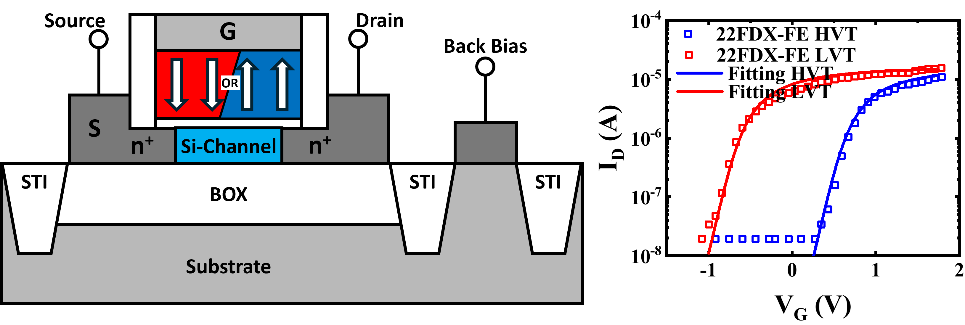
Figure 1: Cross-section and calibrated electrical characteristics of the FDSOI FeFET structure used, demonstrating experimental agreement critical for non-volatile operation.
Control of Vth by the ferroelectric polarization enables binary data encoding. Downward polarization induces Vth,L (logic '1'); upward polarization shifts it to Vth,H (logic '0'), thus the intrinsic memory window (MW) is set by ΔVth=Vth,H−Vth,L.
Bit-cell Architecture and Operation
The proposed 4T differential bit-cell topology consists of two cross-coupled FeFET gain cells and two access NMOS transistors (Figure 2). This structure is a substantial reduction from conventional 6T-SRAM and several hybrid nvSRAM/topologies with larger device counts. Integration into cross-coupled topology ensures robust data retention and enhanced readout via differential sensing.
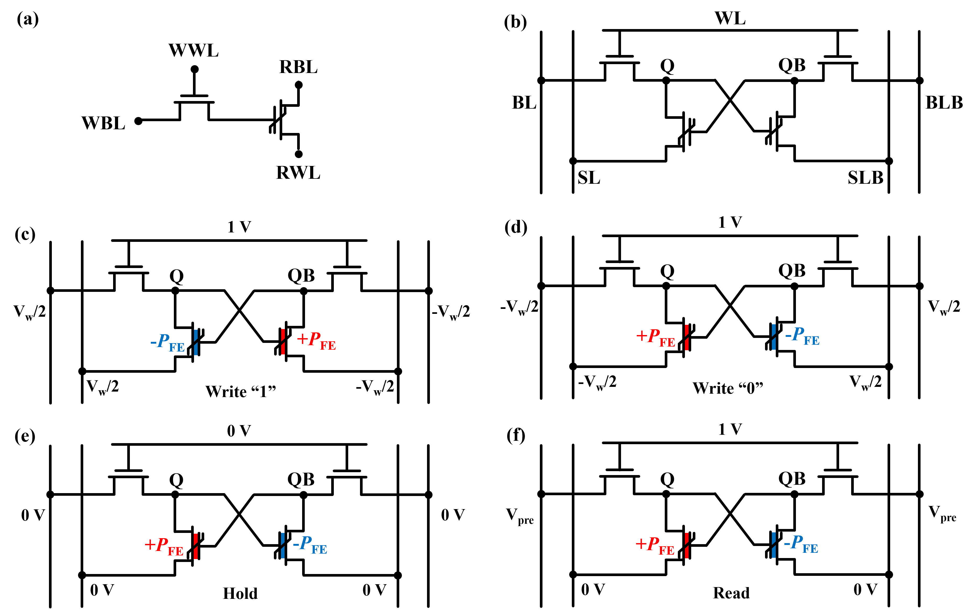
Figure 2: (a) Standard 1T-1FeFET gain cell. (b) Proposed 4T cross-coupled differential bit-cell. (c-f) Write, hold, and read operational waveforms.
Read and write operations are conducted in a voltage-differential scheme on BL/BLB and SL/SLB lines. Write operations employ large voltage differentials to induce Fe polarization, enabling non-volatile state storage. Hold states and read recovery require no sustained power or explicit B/R operations, distinguishing this approach from traditional hybrid-nvSRAM designs. The readout leverages the Vth-driven discharge disparity between NF1 and NF2, compatible with standard differential sense amps.
Integration and Layout Considerations
At the array level, this memory employs periphery compatible with conventional SRAM architectures, with modifications for the negative-voltage write bias required by FeFETs (Figure 3). Differential sense paths and precharge/read circuits are preserved. Layout in GF 22nm demonstrates a compact footprint (1560λ2), confirming the cell-area benefits.
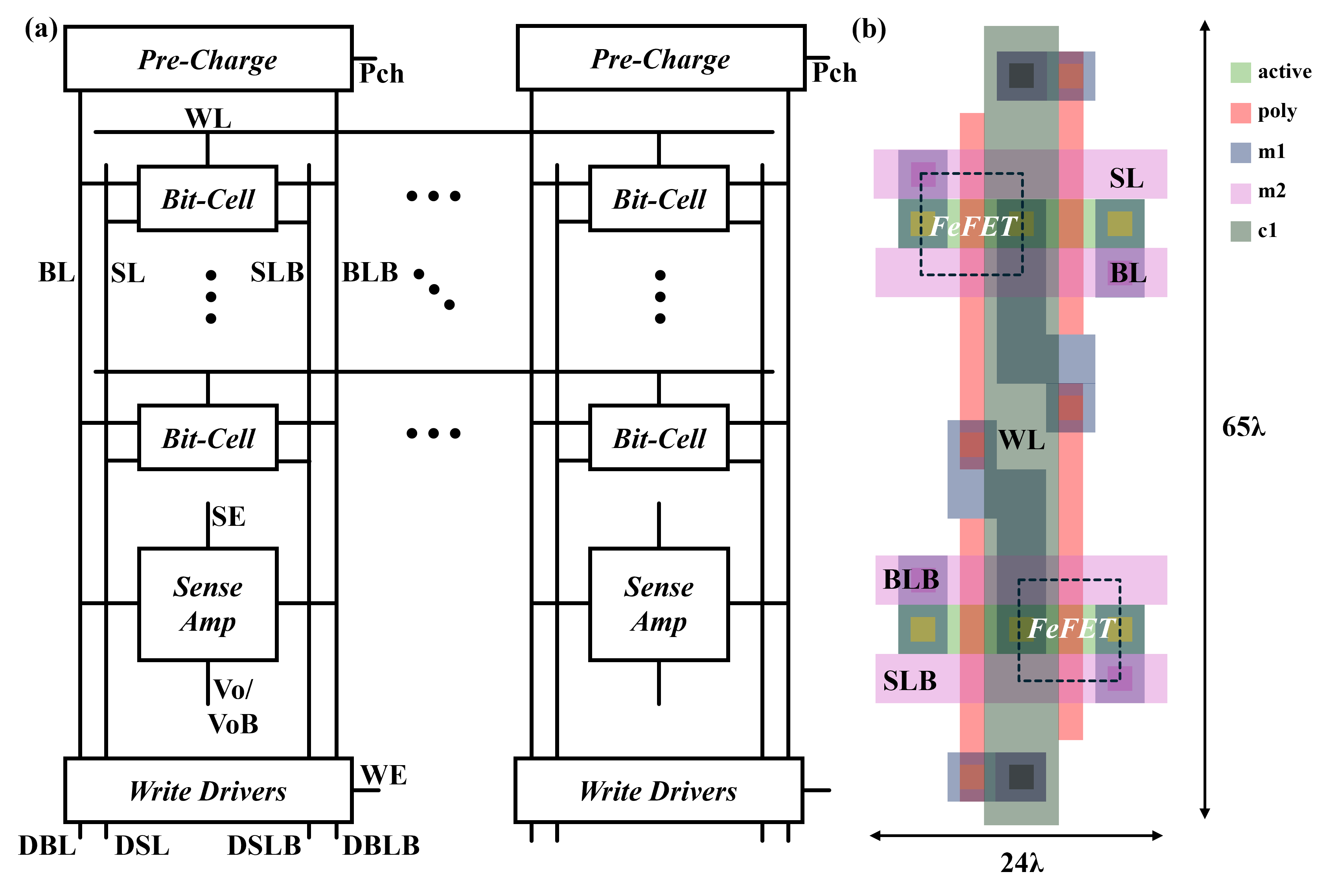
Figure 3: (a) Schematic of the 4T differential bit-cell array with periphery. (b) Physical layout at 22nm node.
Transient Behavior and Hybrid Operating Modes
Transient simulation studies showcase robust store/restore cycles without explicit backup, with program pulse widths as short as 2 ns for reliable storage (Figure 4). The bit-cell transitions seamlessly between volatile and non-volatile operational modes depending on write voltage amplitude. For write voltages Vp≤0.4 V, only volatility is achievable; above this threshold, full non-volatile behavior emerges, making operational mode selection a matter of simple peripheral biasing.
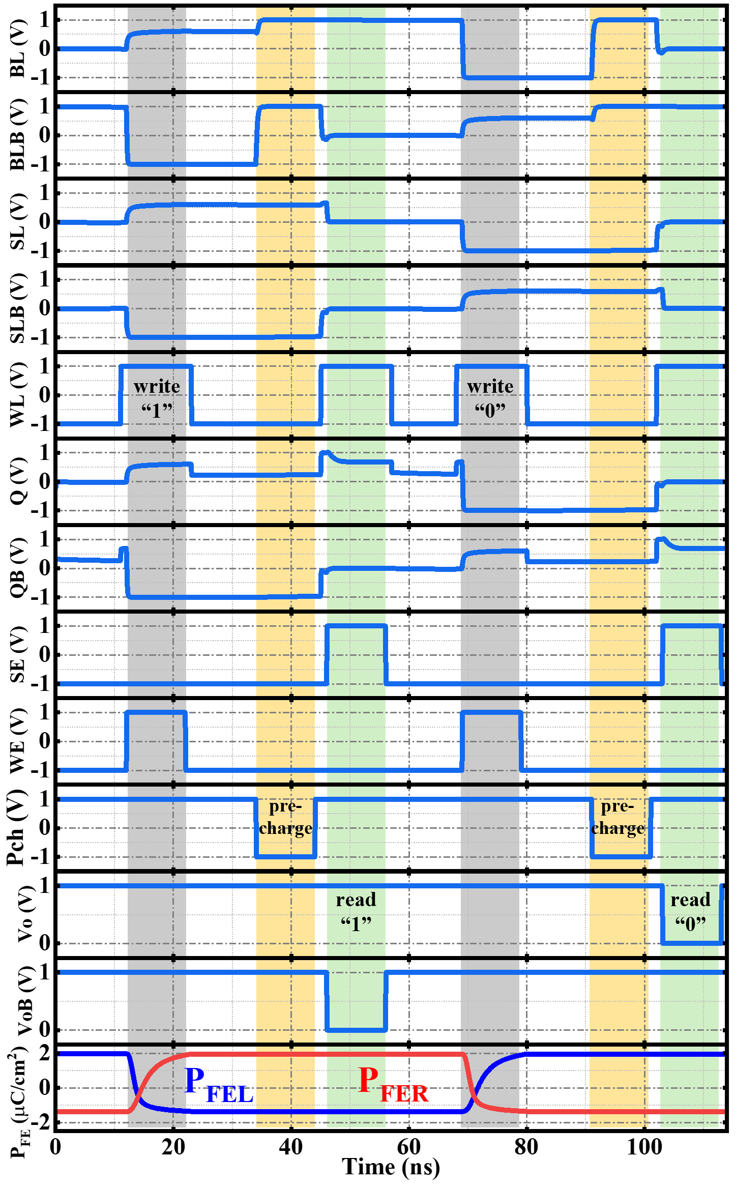
Figure 4: Representative waveforms of write and read cycles validating non-volatile and volatile operational modes across conditions.
Varying write pulse magnitudes and durations reveals clear partitions between volatile (charge domain) and non-volatile (polarization domain) operation regimes (Figure 5, Figure 6). For Vp≥0.6 V and pulse widths tp≥2 ns, the FeFETs reliably program, yielding a robust memory window in read operations. The write energy increases with Vth0, but remains considerably lower than competing eNVM or nvSRAM solutions. Sensing delay is minimized (47 ps non-volatile, 137 ps volatile), and the differential bit-cell demonstrates immunity to moderate write pulse variation, which eases peripheral design constraints.
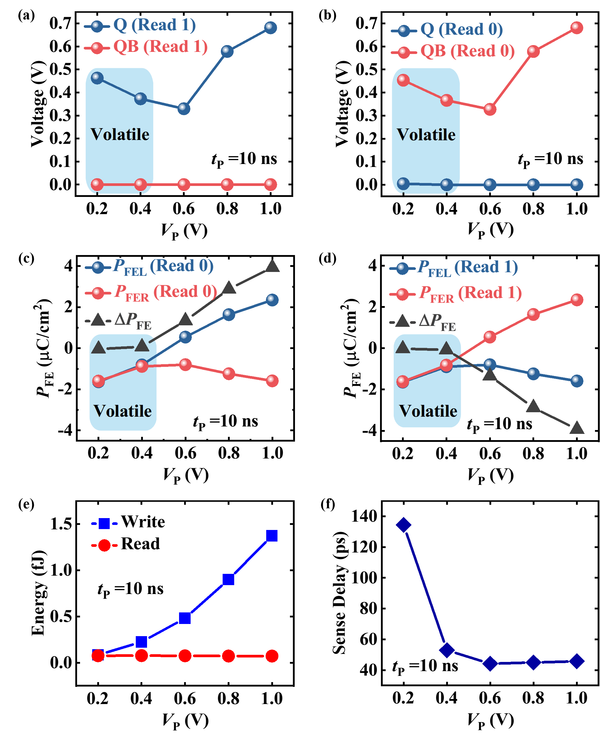
Figure 5: Read-out voltage and polarization tracking under various write voltages, outlining hybrid volatile/non-volatile switching thresholds.
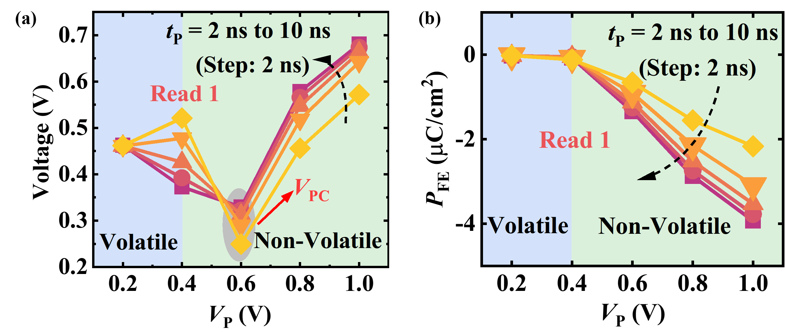
Figure 6: Memory window metrics across the design space—difference in Vth1 (Vth2) and Fe polarization (Vth3) evidencing robust non-volatile storage above critical write pulse thresholds.
Comparative Benchmarking
Compared to state-of-the-art SRAM (6T, 10T) and nvSRAM architectures (e.g., 4T-R, 7T2R, 8T2R), the proposed 4T cell achieves significant reductions in transistor count and area. Notably, the measured store power (0.13 μW) and write time (2 ns) match or surpass prior art. Explicit backup-and-restore (B/R) operations—which substantially degrade standby efficiency in prior schemes—are eliminated without sacrificing non-volatility or endurance expectations.
Practical and Theoretical Implications
The architecture provides a scalable and CMOS-compatible approach for embedded non-volatile memory, directly suitable for IoT and edge applications where stand-by and operational efficiency are paramount. The tunable hybrid memory mode enables adaptation to application-specific requirements, such as fast SRAM-like volatility or deep-sleep retention. Reliance on differential sensing advances integration with contemporary SRAM periphery and supports robust readout in scaled regimes. Device-level endurance and retention, validated by external studies, indicate that the core design will inherit improvements in underlying FeFET technologies without logic-level redesign.
Conclusion
The introduction of a 4T differential FeFET bit-cell with hybrid volatile and non-volatile modes represents a meaningful advancement for embedded memory design, eliminating explicit backup/restore, reducing area, and delivering high-speed, low-power operation with configuration flexibility. The scheme’s compatibility with differential sensing and standard periphery, combined with robust performance across practical design conditions, positions it as a competitive candidate for integration into forthcoming low-leakage, instant-on environments and could serve as a cornerstone for non-volatile compute-in-memory architectures.

