A Cryogenic Uniaxial Strain Cell for Quantum Devices
Abstract: Mechanical strain is a powerful resource for tuning quantum systems, but existing piezoelectric strain cells are generally optimized for fragile, high-aspect-ratio single crystals rather than the thick, square-profile chips typical of semiconductor quantum devices. Furthermore, adapting these cells for qubits requires accommodating dense RF and DC wiring while maintaining strict electrical isolation from high-voltage piezo actuators. Here, we present a piezoelectric uniaxial strain cell designed to homogeneously strain thick, square-profile substrates. We introduce a highly symmetric dual-chip loading configuration that effectively suppresses flexural deformation and shear stress. The cell integrates a high-density RF/DC interposer to support standard wire bonding and encloses the actuators in a grounded Faraday cage to prevent unwanted Stark shifts in the device layer. Finite element simulations confirm that combining stiff actuators with this symmetric mounting drastically improves strain homogeneity. Finally, we validate the apparatus experimentally by applying uniaxial strain to a 200 $μ$m thick silicon die. Surface strain measurements demonstrate an applied strain of 215 $με$ for 200 V applied piezo bias.
Paper Prompts
Sign up for free to create and run prompts on this paper using GPT-5.
Top Community Prompts
Explain it Like I'm 14
What this paper is about
This paper describes a small machine that can gently stretch or squeeze tiny computer chips used for quantum devices while they are extremely cold. The goal is to apply a very even pull in just one direction (called “uniaxial strain”) to chips that are thick and square-shaped, not long and skinny. The device also makes it easy to connect lots of wires for signals and measurements and keeps the chip safe from stray electric fields.
What questions the researchers wanted to answer
- How can we evenly stretch thick, square chips (like those used for quantum computers) without bending them?
- Can we do this at cryogenic temperatures (near absolute zero) and in strong magnetic fields, where quantum devices operate?
- Can we provide lots of safe, high-speed electrical connections while the chip is being strained?
- Will this new design deliver enough, and uniform enough, strain for real quantum experiments?
How the device works (explained simply)
First, a few plain-language definitions:
- Strain: how much something stretches or squeezes compared to its original size. A “microstrain” (µε) is a tiny change: 1 µε = one part in a million.
- Uniaxial: in one direction only.
- Cryogenic: extremely cold.
- Piezoelectric stack actuator: a ceramic “muscle” that gets a little longer or shorter when you apply a voltage.
- Faraday cage: a metal enclosure that blocks electric fields.
What they built and why it helps:
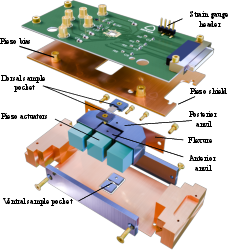
- Three piezo “muscles”: Two on the outside and one in the middle. The middle one moves opposite to the outer pair. Think of three friends pushing and pulling so that the chip in the center gets stretched or squeezed very precisely, without the whole frame moving much. This “three‑stack” setup is compact and works well in strong magnetic fields.
- Extra-stiff parts: They used stiff metals (like molybdenum) and made the piezo stacks thicker. Stiff parts are better at transmitting force to a tough, square chip without losing motion to bending.
- “Sandwich” mounting to stop bending: A square chip tends to bend if you push it from the edges. To fix this, they mount two equal chips—one on top (the device) and one underneath (a “dummy” chip). Like carrying two equally heavy bags, this balances the forces so the chips don’t bend and the strain stays even.
- Better glue contact: The chip sits in a small pocket, and the epoxy (glue) wets the bottom and creeps up the sides. This larger contact area helps pass the strain into the top surface where the device circuits are.
- Lots of safe wiring: A small board (an “interposer”) sits close to the chip with many connection pads. It provides many DC lines and several RF/microwave lines so you can do fast control signals (like those used for spin qubits).
- Electric-field shielding: The high-voltage piezo “muscles” are wrapped in grounded copper, forming a Faraday cage. This keeps their electric fields away from the chip, preventing unwanted “Stark shifts” (accidental changes in the chip’s energy levels).
- Guided motion without friction: A copper “flexure” guides the moving parts smoothly, avoiding sliding parts that could stick or wear out during cooling and heating.
How they checked it:
- Computer simulations: They used finite element analysis (FEA), which is like a detailed virtual crash-test for the chip and metal parts. To model the piezos simply, they used a standard trick that treats their expansion like thermal expansion (as if they were “heating up” to grow).
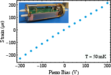
- Real measurements: They glued a tiny strain gauge (a sensor that changes resistance when stretched) onto a silicon chip and cooled the whole setup to 50 millikelvin (that’s 0.05 degrees above absolute zero). By changing the voltage on the piezos and reading the gauge, they measured how much strain the chip actually felt.
What they found and why it matters
Main results:
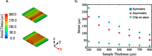
- Even strain across the chip: With the “two-chip sandwich” mounting, the strain variation in the central 1×1 mm area dropped from about 53% (bad) to about 5% (good). That means the surface strain is very uniform—important for accurate calibration and for devices that span this area.
- Enough strain for quantum devices: At 200 V on the piezos, they reached about 215 µε (microstrain). Their measurements were nicely linear: about 1.085 µε per volt. With higher safe voltages at low temperatures, the same setup could reach around 600 µε (0.6 millistrain) without special chip shaping.
- Works for thick chips: Simulations show you still get useful, fairly uniform strain even for chips up to 800 µm thick, similar to some silicon/germanium platforms used for spin qubits.
- Better than simple methods: Compared to the common shortcut of gluing a chip directly onto a piezo face, this design delivers more strain per volt and keeps the strain more uniform across the chip’s surface.
- Cryogenic note: The piezo “muscles” shrink in effectiveness when very cold, keeping only about 5.8% of their room‑temperature motion at 50 mK. Even so, the device delivers the needed strain. Future piezo materials could improve this further.
Why this is important:
- Many proposed quantum‑chip improvements need only a few hundred microstrain to reach “sweet spots” that make the qubits more stable or easier to control. This device achieves that range while keeping the chip fully connected and shielded—exactly what experiments require.
What this could change going forward
This strain cell lets researchers:
- Tune real quantum chips (not just fragile lab samples) by stretching them evenly and safely at ultra‑low temperatures.
- Keep using standard wire bonding and fast control lines, so the strained chip can run full quantum experiments.
- Explore predicted strain “sweet spots” for silicon spin qubits, possibly improving gate speeds, reducing noise, and boosting fidelity.
- Study how mechanical strain affects advanced materials and device physics without redesigning the chip.
In short, the team built a practical, low‑temperature “stretching tool” for modern quantum chips that keeps the strain even, the wiring plentiful, and the device protected—opening the door to new experiments and better-performing quantum hardware.
Knowledge Gaps
Below is a single, consolidated list of concrete knowledge gaps, limitations, and open questions that remain unresolved in the paper. Each point is phrased to be actionable for future work.
- Actuation at millikelvin temperatures: The PZT stacks retain only 5.8% of room‑temperature stroke at 50 mK; the paper suggests alternatives (e.g., SrTiO3, alternative PZT compositions) but does not quantify their low‑T stroke, hysteresis, creep, or long‑term stability across the full cryogenic range (300 K → 10 mK).
- High‑voltage limits at base temperature: Performance, leakage, dielectric breakdown, and heating of stacks and cabling at ≥600 V and 50 mK are not tested; safe operating margins, corona onset in vacuum, and reliability under sustained biases remain unknown.
- Closed‑loop control and calibration: The cell lacks integrated displacement/force sensing; the voltage‑to‑strain transfer function depends on mount and epoxy; no approach is demonstrated for in situ closed‑loop strain control or for per‑mount calibration to mitigate sample‑to‑sample variation.
- Dynamic bandwidth and noise: Only quasi‑static operation is assessed; frequency response, resonance modes, mechanical Q, microphonics, and strain noise spectra at mK (including coupling to qubit‑relevant frequency bands) are uncharacterized.
- Thermal load at mK: The added thermal load from high‑voltage piezo operation and RF drive (bias‑tees up to ~100 MHz, ESR line 3.5–7.5 GHz) is not quantified; resultant temperature rise, thermal gradients, and heat‑sinking efficacy for the chip and interposer are unmeasured.
- Magnetic‑field operation: Although designed for ±8 T, the apparatus is not tested in field; potential issues from eddy currents, Lorentz forces on RF/DC conductors, magnetostriction, and field‑dependent actuator behavior during ramps remain unaddressed.
- Strain homogeneity validation: Homogeneity is inferred from FEA; there is no experimental strain mapping (e.g., low‑T micro‑Raman, XRD, or DIC) to verify the simulated ~5% inhomogeneity across mm‑scale chips.
- Inhomogeneity metric definition: The equation for the strain inhomogeneity Δ appears typeset incorrectly, making the exact definition ambiguous; a clear, reproducible metric and ROI selection protocol are needed.
- Sensitivity to assembly tolerances: The impact of epoxy bondline thickness variation (nominally ~100 μm), bondline modulus dispersion, and anvil/sample misalignment on strain transfer and homogeneity is not quantified via sensitivity analysis or experiment.
- Epoxy properties at cryo: The assumed cryogenic elastic properties of Stycast 2850 are literature‑based; direct low‑T characterization (Young’s/shear moduli, loss tangent) for the exact cure profile, thickness, and aging under thermal cycling is lacking.
- Epoxy/adhesive reliability: Long‑term durability, debonding thresholds, and performance after repeated high‑voltage actuation and multiple cooldowns are not tested; failure modes at chip/epoxy/anvil and actuator/anvil interfaces remain undefined.
- Symmetric dual‑chip mounting robustness: The homogeneity benefit assumes identical dummy/device chips; tolerance to thickness, elastic modulus, CTE mismatches, and partial asymmetry is not studied; guidance is needed for cases where a matching dummy is unavailable.
- Through‑thickness strain gradients: While the authors argue volume inhomogeneity is irrelevant for surface devices, vertical gradients through the substrate and their influence on near‑surface device layers (e.g., shallow quantum wells) are not quantified experimentally.
- Substrate/material dependence: Validation is only on 200 μm Si strained along [110]; performance and homogeneity for other substrates (e.g., SiGe, GaAs, sapphire), thicker wafers (up to 800 μm predicted), and anisotropic/heterostructured stacks are untested.
- Local vs global strain at device features: Effects of patterned metal gates, oxides, and topography on local strain transfer to nanoscale quantum devices are not measured; possible strain shielding or stress concentration near features remains unknown.
- Maximum force/stress and fracture risk: The actual force delivered to the chip and stress safety margins relative to fracture thresholds are not established; without a force sensor, fragile devices risk damage during actuation.
- Out‑of‑plane bending/tilt: Although the symmetric configuration should suppress bending, no direct metrology (e.g., interferometry) verifies out‑of‑plane tilt/rotation of the anvils/chips under load.
- Strain transfer efficiency discrepancy: Simulations overpredict strain by ~20%; the specific contributions of each interface (piezo–anvil, anvil–plate, plate–epoxy–chip, gauge adhesive) to loss are not deconvolved; improved models or measurements are needed.
- EMI and electric‑field isolation: The Faraday cage concept is described but not quantified; no measurements of stray electric fields at the device plane, capacitive feedthrough from piezo leads, or charge noise on DC gates during piezo operation are provided.
- RF/microwave performance at mK: The interposer’s S‑parameters (insertion/return loss, crosstalk), ESR line power handling, and bias‑tee performance at cryo and in field are not characterized; RF‑induced heating and interference with piezo operation are unknown.
- Crosstalk and shielding between RF/DC and piezo drives: Isolation between high‑voltage piezo cables and sensitive RF/DC lines is not measured (e.g., via network analysis or noise tests) under realistic operating conditions.
- Wire‑bond reliability under strain: The effect of repeated actuation on bond‑wire fatigue, bond‑pad integrity, and loop‑height optimization is not assessed; acceptable actuation ranges and cycle counts for reliable operation remain to be determined.
- Device‑level validation: No demonstration is provided on actual qubit devices (e.g., coherence times, gate fidelities, “sweet‑spot” tuning) under applied strain; quantifying strain‑induced improvements or degradation in qubit performance is an open task.
- Alignment to crystallography: Procedures and tolerances for aligning the strain axis to device/crystal axes on real chips (and the impact of misalignment on homogeneity and device response) are not defined.
- Scaling of wiring density: The interposer provides 14 DC and 5 RF lines; strategies and limits for scaling to the tens/hundreds of lines needed by multi‑qubit arrays while preserving strain homogeneity and isolation are not explored.
- Vibration coupling to cryostat: The mass, mechanical anchoring, and vibrational coupling of the cell to the mixing‑chamber plate are not discussed; how cell resonances couple to the cryostat and to devices is unknown.
- Thermal contraction and preload strategy: Brass fasteners provide additional preload upon cooldown; quantitative control of preload, its variability, and its effect on strain transfer and actuator stress (including at 8 T with possible eddy current heating) are not assessed.
- Piezo drive protocols: Hysteresis, creep, and drift of the three‑stack actuator at mK under typical scan/hold protocols are unreported; optimal drive waveforms and compensation schemes for stable strain setpoints need development.
- Field‑ramp transients: The response of the cell and wiring during rapid magnetic‑field changes (induced voltages, heating, mechanical forces) is not characterized; operating envelopes for magnet use remain undefined.
- Strain gradient near edges/epoxy meniscus: Edge effects and strain concentrations near epoxy boundaries are not quantified; safe die geometries, fillets, and pocket designs to minimize cracking require study.
- Parametric design rules: Apart from a single bondline thickness and actuator selection, there is no parametric map or design chart linking actuator stiffness, anvil material/geometry, bondline properties, and chip dimensions to expected strain/homogeneity.
- Documentation of assembly reproducibility: The paper presents a single successful build; statistical data over multiple assemblies/cooldowns on transfer efficiency, homogeneity, and failure rates are missing.
- Compatibility with different measurement setups: Integration constraints (space, connectors, heat‑sinking) for common cryostats and magnet bores are not fully specified; a mechanical/thermal interface standard would aid adoption.
These gaps point to concrete follow‑up experiments, component characterizations, and design refinements that would rigorously validate the cell for strained quantum‑device studies and guide broader deployment.
Practical Applications
Immediate Applications
The following items translate the paper’s results into deployable use cases, with sectors, potential tools/products/workflows, and feasibility notes.
- [Industry | Quantum computing | Test & Measurement] Chip-level strain tuning and screening of Si/SiGe spin qubits
- Use case: Rapidly map “strain sweet spots” (e.g., for acceptor-based qubits) by sweeping uniaxial strain while measuring EDSR frequencies, g-tensors, valley splitting, and coherence.
- Tools/products/workflows: This strain cell as a cryostat add-on; automated HV piezo control synchronized with qubit measurement software; integrated strain-gauge calibration workflow using the reported 1.085 με/V slope; use of the RF/DC interposer (14 DC, 5 RF with integrated bias tees to ~100 MHz plus an ESR line at 3.5–7.5 GHz).
- Assumptions/dependencies: Dilution refrigerator access; HV piezo supply up to 200–600 V; availability of dummy chips for symmetric loading; cryo-compatible epoxies (Stycast 2850) with ~100 μm bondlines; acceptance of 5.8% residual piezo stroke at 50 mK (or substitution with lower temperature-dependence actuators later).
- [Academia | Condensed-matter physics | Superconductivity] Device-style transport and microwave experiments under homogeneous uniaxial strain on square, thick substrates
- Use case: Strain-tuned studies of nematicity, charge-density waves, and superconductivity on chips that must host dense RF/DC wiring (e.g., cuprates, ruthenates, iron pnictides) without resorting to fragile beam geometries.
- Tools/products/workflows: The symmetric dual-chip mounting that reduces surface strain inhomogeneity to ~5% across a 1×1 mm² ROI; molybdenum anvils and stiff actuators to ensure efficient strain transfer; copper blade flexure for reproducible motion; lock-in metrology of strain via surface gauges.
- Assumptions/dependencies: Nonmagnetic bill of materials for operation up to ±8 T; careful epoxy sidewall wetting to enhance strain transfer; validated FEA (thermal–piezo analogy) for sample-specific mounting geometries.
- [Industry & Academia | Packaging & Cryo-RF engineering] Faraday-caged high-voltage piezo actuation to prevent stray-field-induced Stark shifts
- Use case: Electrically quiet cryo-packaging for quantum devices by enclosing actuators in a grounded copper shield and using isolated SMPM piezo feeds.
- Tools/products/workflows: Reference design for HV delivery (un-attenuated stainless-steel coax to shielded SMPM connectors) and a grounded copper enclosure that decouples actuator fields from device layers.
- Assumptions/dependencies: Meticulous ground design across PCB interposer, shield, and cryostat; adherence to cryo HV safety practices.
- [Industry | Semiconductor manufacturing R&D | Yield engineering] Correlating process-induced strain/disorder with device performance
- Use case: Screen lot-to-lot or across-chip process variation by externally tuning uniaxial strain and measuring device sensitivity (e.g., operating voltages, dot formation thresholds, disorder-dot likelihood).
- Tools/products/workflows: Strain sweeps coupled to automated device characterization; integration into fab feedback loops; structured DOE across chip orientations ([110], [100]).
- Assumptions/dependencies: Availability of mm-scale diced chips (not full wafers); robust wire bonding within ~1 mm of strained die.
- [Academia | Quantum sensing & spin physics] Controlled studies of strain–hyperfine and spin–phonon coupling in donor/acceptor systems
- Use case: Validate and extend predictions for tunable strain-enhanced EDSR and noise sweet spots; probe nuclear acoustic resonance regimes with static bias strain plus RF drive lines.
- Tools/products/workflows: Use of the 3.5–7.5 GHz ESR line and bias-tee RF/DC lines; symmetric mounting to minimize bending-induced gradients that confound calibration.
- Assumptions/dependencies: Device designs targeting acceptor/donor states; accurate strain calibration on the same chip area as the quantum device.
- [Policy & Standards | Lab safety, EMI/ESD] Best practices for cryogenic HV isolation and EMI containment in quantum cryostats
- Use case: Establish internal lab or consortium guidelines for HV delivery and shielding around piezo-driven tuners to avoid unintended Stark shifts and charge rearrangements.
- Tools/products/workflows: Documented SMPM isolation, grounded enclosures, and line routing; checklists for dilution-refrigerator HV operation.
- Assumptions/dependencies: Institutional buy-in; alignment with existing cryo and electrical safety policies.
- [Education | Graduate instrumentation training] Hands-on modules in cryogenic actuation, strain metrology, and RF/DC cryo-packaging
- Use case: Train students in building and operating strain-tuning hardware compatible with modern quantum-device wiring.
- Tools/products/workflows: Course lab kits using the dual-chip mounting concept, FEA thermal–piezo analogy templates (e.g., MSC/NASTRAN), and strain-gauge calibration protocols.
- Assumptions/dependencies: Access to low-temperature infrastructure; institutional safety approvals for HV.
Long-Term Applications
These opportunities likely require further research, scaling, or engineering development before deployment.
- [Industry | Quantum processors] On-package, closed-loop strain control for multi-qubit arrays
- Use case: Actively trim qubit parameters (e.g., valley splitting, g-factors) across arrays to equalize operating points and suppress variability.
- Tools/products/workflows: Next-gen actuators with higher cryo stroke (e.g., SrTiO3 or modified PZT), integrated displacement/force/strain sensing, feedback control; compact Faraday-caged actuators in multichip modules.
- Assumptions/dependencies: Miniaturization compatible with qubit pitch; thermal budget and vibration isolation in dilution refrigerators; reliability of epoxies or alternative clamps over many thermal cycles.
- [Industry & Academia | Wafer-scale characterization] Strain-enabled wafer probing at 1–4 K for yield and variability studies
- Use case: Extend 300 mm cryo probing to include controlled uniaxial strain for rapid mapping of strain sensitivities across wafers.
- Tools/products/workflows: Scalable strain stages with high stiffness and homogeneity over die-sized fields; robotic alignment; high-voltage distribution with wafer-prober safety interlocks.
- Assumptions/dependencies: Mechanical redesign for wafer-scale loads; standardization of die pockets; compliance with industrial tool footprints.
- [Academia | Quantum control research] Dynamic strain as a control primitive for gates and coupling
- Use case: Parametric modulation of spin–phonon coupling, strain-mediated two-qubit gates, and noise spectroscopy using AC strain.
- Tools/products/workflows: High-bandwidth, low-vibration piezo stacks; co-design of mechanical resonances with qubit frequencies; precision EMI shielding to prevent electric-field crosstalk.
- Assumptions/dependencies: Actuator bandwidth and stability at mK; mitigation of microphonics; co-integration with superconducting wiring.
- [Industry | Reliability & Qualification] Cryogenic mechanical-stress qualification standards for quantum ICs
- Use case: Define JEDEC-like standards for allowable stress/strain cycles, epoxies, and mounts specific to quantum chips and cryo operation.
- Tools/products/workflows: Reference fixtures based on the symmetric dual-chip concept; standardized strain-calibration coupons; reporting formats for strain homogeneity (e.g., ≤5% over 1×1 mm² ROI).
- Assumptions/dependencies: Cross-industry consortium support; round-robin inter-lab validation.
- [Software & Design Automation] PDK-integrated strain-aware design and FEA toolchains
- Use case: Include strain transfer, homogeneity, and CTE-mismatch models in quantum PDKs to predict device performance under package-induced or intentional strain.
- Tools/products/workflows: Open-source FEA templates using the thermal–piezo analogy; CAD libraries for recessed pockets, sidewall-wetting epoxy geometries; digital twins for sample–mount assemblies.
- Assumptions/dependencies: Availability of reliable cryogenic material properties (Young’s/shear moduli, CTE) for epoxies and substrates.
- [Policy & Standards | EMI/ESD and HV] Formal standards for HV piezo operation in cryogenic quantum systems
- Use case: Codify shielding, grounding, connector isolation (e.g., SMPM), and allowed field emissions near sensitive device layers.
- Tools/products/workflows: Standards documents, certification procedures, and compliance tests (field-leakage measurements, Stark-shift thresholds).
- Assumptions/dependencies: Engagement from standards bodies and national labs; alignment with cryogenic safety frameworks.
- [Cross-sector translation | Consumer and industrial electronics testing] Symmetric dual-fixture strategies to suppress bending in room-temperature strain tests of PCBs and MEMS
- Use case: Apply the dual-sample (or dummy-substrate) concept to improve strain homogeneity in benchtop fixtures for reliability testing.
- Tools/products/workflows: Fixture designs that balance bending moments using matched-stiffness counter-samples; sidewall-adhesion strategies to improve strain transfer.
- Assumptions/dependencies: Adaptation to non-cryo environments and different materials; validation with optical/DIC strain mapping.
- [Big science instrumentation | Particle physics, astronomy] Strain-tuning of cryogenic sensors and materials
- Use case: Explore performance tuning of cryogenic sensors (e.g., TES, KIDs) and superconductors via homogeneous strain without introducing electric-field noise.
- Tools/products/workflows: Faraday-caged actuators integrated into low-background cryogenic instruments; calibrated strain delivery to thick substrates.
- Assumptions/dependencies: Mechanical integration with vibration-sensitive detectors; compatibility with ultra-low-noise readout chains.
Notes on feasibility across applications:
- Performance presently limited by cryogenic piezo stroke (~5.8% of room temperature); adoption of temperature-stable actuators (e.g., STO or tailored PZT) increases headroom.
- Strain homogeneity and transfer rely on symmetric loading with matched-stiffness “dummy” chips, recessed pockets, and sidewall-wetted epoxy; deviations (thickness mismatch, bondline variance) reduce uniformity.
- HV safety, EMI control, and nonmagnetic construction are essential for operation up to ±8 T and mK temperatures.
- Vibration and microphonics must be managed for any dynamic-strain applications intended for quantum control.
Glossary
- acceptor spin states: Bound hole states associated with acceptor dopants in semiconductors that can participate in qubit operations. "while controlled local strain can couple directly to donor or acceptor spin states, tune hyperfine interactions, and mediate spinâphonon coupling."
- anvils: Rigid pads that transmit force/strain to the sample in a strain cell. "The anvils are guided relative to the cell body by a copper blade flexure."
- band-pass response: A filter characteristic allowing signals within a certain frequency range to pass while attenuating frequencies outside that range. "with a band-pass response with a $3.5$â passband, suitable for microwave manipulation of spin qubits or other resonant excitations."
- bias tees: RF components that combine or separate DC and RF signals on a single line. "Four of the RF lines are integrated with on-board bias tees, allowing combined DC and RF excitation up to for gate and control signals."
- bondline: The layer of adhesive between two bonded parts, whose thickness affects mechanical coupling. "with a measured bondline thickness of approximately 100 m"
- clamping preload: An intentional compressive force applied by the assembly to maintain contact and stiffness, especially across thermal cycles. "provides an additional clamping preload on the internal components during cooldown."
- coefficient of thermal expansion (CTE): The fractional change in size of a material per unit temperature change. "the coefficient of thermal expansion (CTE) of Mo () is very well matched to the transverse CTE of the PZT actuators it is bonded to"
- dilution refrigerator: An ultra-low-temperature cryostat that achieves millikelvin temperatures using a mixture of helium-3 and helium-4. "operate in a dilution refrigerator in large in-plane magnetic fields"
- dual-chip loading configuration: A symmetric mounting scheme using a second, dummy chip to balance loads and suppress bending. "We introduce a highly symmetric dual-chip loading configuration that effectively suppresses flexural deformation and shear stress."
- electric-dipole spin resonance (EDSR): A technique to drive spin transitions using electric fields via spin–orbit coupling. "support microwave electric-dipole spin resonance (EDSR) drive lines"
- elastocaloric: Pertaining to temperature/entropy changes induced by applied strain. "revealed strong elastoresistive and elastocaloric signatures in correlated metals"
- elastoresistive: Pertaining to changes in electrical resistance due to applied strain. "revealed strong elastoresistive and elastocaloric signatures in correlated metals"
- Faraday cage: A conductive enclosure that shields its interior from external electric fields. "This geometry forms an electrostatic Faraday cage around the actuators and ensures that the quantum device sees only the intended gate and bias potentials."
- Fermi surfaces: Surfaces in momentum space separating occupied from unoccupied electron states at zero temperature; their shape governs electronic properties. "reshape Fermi surfaces, and selectively couple to nematic, superconducting, or density-wave order parameters."
- finite element analysis (FEA): A numerical method for solving complex mechanical or physical field problems by discretizing the domain into elements. "We therefore assess the strain distribution using three-dimensional finite element analysis (FEA) in NASTRAN"
- flexure: A compliant, hinge-like mechanical element that guides motion without sliding friction. "The anvils are guided relative to the cell body by a copper blade flexure."
- g-tensors: Anisotropic generalizations of the electron g-factor describing how spins couple to magnetic fields in solids. "influences effective g-tensors"
- hyperfine interactions: Couplings between electron and nuclear spins that affect qubit energy levels and coherence. "tune hyperfine interactions"
- interposer: An intermediate substrate or board used to route dense electrical connections close to a device. "A high-density RF/DC interposer is mounted directly above the strained chip, with bond pads located within roughly of the sample surface"
- lock-in techniques: Phase-sensitive detection methods that extract small signals at a reference frequency from noisy backgrounds. "which is measured via standard lock-in techniques"
- millistrain: A strain unit equal to 10-3 (one part per thousand). "reported strains on the order of 10 millistrains."
- NASTRAN: A finite element analysis software package used for structural and related simulations. "We therefore assess the strain distribution using three-dimensional finite element analysis (FEA) in NASTRAN"
- nematic: Referring to phases that break rotational symmetry without breaking translational symmetry. "selectively couple to nematic, superconducting, or density-wave order parameters."
- nematic superconductivity: A superconducting state that spontaneously breaks rotational symmetry of the crystal lattice. "enabled controlled studies of nematic superconductivity"
- order parameter: A quantity that characterizes the degree of symmetry breaking across a phase transition. "selectively couple to nematic, superconducting, or density-wave order parameters."
- passband: The frequency range over which a filter or circuit passes signals with minimal attenuation. "with a band-pass response with a $3.5$â passband"
- piezoelectric stack actuators: Layered piezoelectric devices that expand or contract under applied voltage to produce precise motion or force. "two outer piezoelectric stack actuators flank a central stack along the strain axis"
- poling direction: The orientation of the aligned electric dipoles in a poled piezoelectric material that sets its primary actuation axis. "their expansion along the poling direction during cooldown"
- PZT actuators: Piezoelectric actuators made from lead zirconate titanate (PZT), a common piezo ceramic. "the transverse CTE of the PZT actuators it is bonded to"
- quasi-static operation: Operating conditions where changes occur slowly enough that dynamic effects (inertia) can be neglected. "where the quasi-static operation of the piezoelectric actuators is modeled via a thermal-expansion analogy"
- region of interest (ROI): A defined subarea of a sample or image chosen for focused analysis. "Axial strain at the center of the 1Ã1 mm² region of interest"
- shear modulus: A material property quantifying resistance to shear deformation. "a Young's and Shear modulus of 16 GPa and 6 GPa respectively for the Stycast 2850"
- shear stress: A stress component parallel to a material surface that tends to cause layers to slide relative to each other. "effectively suppresses flexural deformation and shear stress."
- SMPM connectors: Miniature RF coaxial connectors used for high-frequency signal transmission. "terminated in shielded SMPM connectors that feed directly into the strain cell."
- spin–phonon coupling: Interaction between electron spin states and lattice vibrations that can affect qubit dynamics. "mediate spinâphonon coupling."
- Stark shifts: Shifts in energy levels of a system due to applied electric fields. "to prevent unwanted Stark shifts in the device layer."
- strain amplification: An effect where the mechanical arrangement multiplies the strain delivered to a sample compared to direct actuation. "as a result of the ``strain amplification" effect provided by actuating the anvils."
- strain gauge: A sensor whose resistance changes with strain, used to measure deformation. "monitoring the strain of one of the piezo actuators via an epoxied strain gauge."
- strain homogeneity: The uniformity of strain across a sample’s area, important for reliable device characterization. "increase strain homogeneity and throughput"
- thermal-expansion analogy: A modeling approach that represents piezoelectric actuation as equivalent thermal expansion in finite element simulations. "modeled via a thermal-expansion analogy where the piezoelectric coefficients are mapped to the thermal expansion coefficients."
- three-stack geometry: A piezo-driven strain-cell layout using two outer stacks and one central stack driven differentially for compact, precise actuation. "piezoelectric stacks arranged in a compact, differential âthree-stackâ geometry"
- uniaxial strain: Strain applied along a single axis, producing directional deformation. "By breaking crystal symmetries and modifying bond angles and bond lengths, uniaxial strain can drive or enhance phase transitions"
- valley splitting: The energy separation between equivalent minima (valleys) in a semiconductor’s conduction or valence band structure. "epitaxial strain in quantum wells and heterostructures sets valley splitting, modifies band offsets, and influences effective g-tensors"
- wire bonding: A method of making electrical interconnections to a chip using fine wires (e.g., gold or aluminum). "to support standard wire bonding"
- Young's modulus: A material’s stiffness, defined as stress over strain in the elastic regime for uniaxial loading. "a Young's and Shear modulus of 16 GPa and 6 GPa respectively for the Stycast 2850"
Collections
Sign up for free to add this paper to one or more collections.