- The paper demonstrates that micro-transfer printing achieves over 95% yield and sub-500 nm alignment accuracy for integrating TFLN modulators.
- The process utilizes pre-patterned TFLN coupons on SiPho platforms to produce modulators with <2 dB insertion loss and >70 GHz electro-optic bandwidth.
- The scalable, CMOS-compatible integration paves the way for next-generation data center interconnects and heterogeneous photonic device platforms.
Introduction and Background
Silicon photonics (SiPho) is at the forefront of photonic integrated circuit (PIC) development for data center and AI workloads, driven by the imperatives of energy efficiency, bandwidth scalability, and integrability with CMOS foundries. However, state-of-the-art depletion-mode silicon modulators confront intrinsic trade-offs in bandwidth, drive voltage, and optical loss, rendering them suboptimal for high-speed optical interconnects and analog applications. Thin-film lithium niobate (TFLN) has emerged as a promising solution, attributable to its high electro-optic (EO) coefficient, low-loss propagation, and capacity for GHz-range modulation bandwidths. Yet, TFLN is not CMOS-compatible due to lithium contamination, which impedes its native integration into mature silicon foundry flows and compels the pursuit of hybrid and heterogeneous integration strategies [(2605.28971, Lin et al., 4 May 2026), niels_high-speed_2026].
Wafer-to-wafer and die-to-wafer bonding have enabled pathways for heterogeneous SiPho-TFLN integration but suffer from inefficiencies such as wafer-wide material consumption, process-incompatibility, and scalability bottlenecks. Micro-transfer printing (MTP) has recently garnered attention as a versatile manufacturing technique for the precise, efficient placement of die-sized functional films ("coupons") onto processed wafers, enabling known-good-die integration and flexibility in process scheduling [niels_advances_2026, roelkens_present_2024, chen2026micro]. The present work demonstrates the utility and scalability of MTP for integrating pre-patterned TFLN modulators, specifically Mach–Zehnder modulators (MZM), on 200-mm SiPho wafers, reporting over 95% device yield and sub-500 nm (3σ) alignment accuracy across four complete wafers.
The demonstrated workflow uses commercially available wafer-scale MTP tools compatible with 200-mm and 300-mm wafers. Pre-structured TFLN devices, with tapers and etched waveguides, are fabricated on a source wafer, released via under-etch, and subsequently retrieved and placed using a PDMS stamp onto target SiPho wafers. The automation of coupon retrieval, placement, and in-situ alignment feedback enables high reproducibility and efficiency at the die level. Integration is performed on passive SiN/Si waveguide platforms, with optical coupling transitions designed for low modal loss. Post-transfer, redistribution layers (RDL) for metal electrodes are defined via back-end processing.
This work transitions from early-generation slab-based TFLN coupons to patterned, waveguide-based coupons with optimized tapers, yielding improved mode confinement and stronger EO interaction. As a result, the devices allow for narrower electrode gaps and more aggressive Vπ reduction.
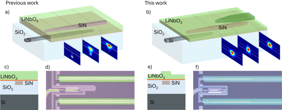
Figure 1: Structural and optical design comparison between prior slab-based TFLN MTP integration and the present patterned, waveguide-based approach, showing enhanced mode confinement and practical cross-sections.
Wafer-Scale Throughput, Alignment, and Yield
Four 200-mm wafers were populated with more than 600 phase modulators (≥95% yield), corresponding to 300 amplitude modulators per wafer. The MTP process achieved 3σ alignment accuracy of 420 nm in the critical y-axis, vital for minimizing insertion loss at waveguide interfaces. Statistical characterization reveals a Gaussian spread of the misalignment error and demonstrates process refinement from run to run. Printing failures are primarily ascribed to inhomogeneities in coupon preparation and wafer handling, suggesting further improvements with fully automated inspection and quality assurance.
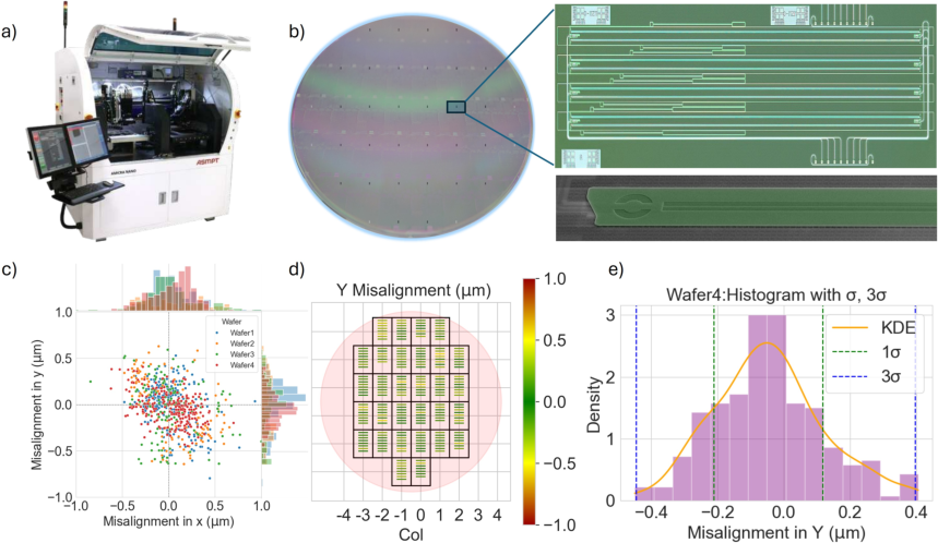
Figure 2: Wafer-scale MTP platform, printing alignment statistics for four wafers, and spatial distribution of y-axis misalignment, illustrating robust coupon placement uniformity over the wafer.
Optical and Electro-Optic Device Characterization
Wafer-level automated probing establishes the optical performance of more than 600 devices. Insertion loss (IL) is typically <2 dB, with statistical uniformity correlated to local placement accuracy. Extinction ratios exceeding 30 dB confirm high MZM interferometric quality.
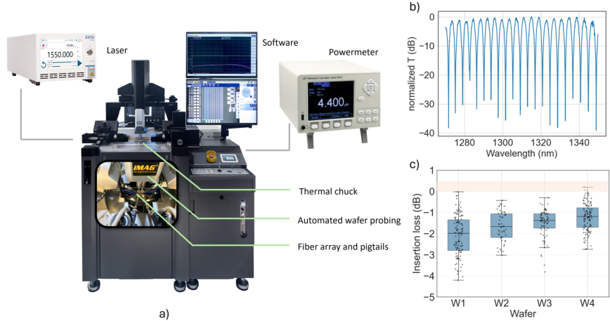
Figure 4: Automated wafer-scale characterization setup, typical transmission spectrum of a normalized MZM, and statistical IL metrics across four wafers showing sub-2 dB mean IL.
For active device assessment, post-MTP metallization (500 nm Al, with 100 nm oxide spacer) forms ground-signal-signal-ground (GSSG) electrodes. Electrode gaps between 4–6 μm are investigated, with empirical Vπ ranging from ~4 V upward, demonstrating the expected linear dependence with gap width. However, the metal layering process introduces additional IL (~2 dB), primarily due to limitations in alignment precision, which could be mitigated by enhanced RDL lithography such as stepper-based exposure or co-printed electrodes.
On selective chips, the platform supports high-speed EO response: for 1 μm-thick Al electrodes, measured small-signal EOE (electrical-optical-electrical) bandwidth exceeds 70 GHz, while thinner (500 nm) electrodes are limited to 20–30 GHz—this bandwidth is predominantly dictated by metal electrode design and wafer resistivity rather than intrinsic material or device constraints.
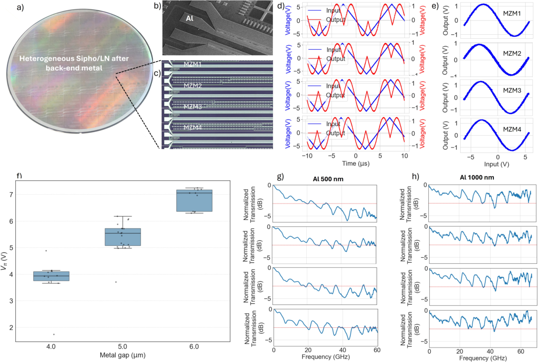
Figure 6: Electro-optic test configuration, metallized device images, typical RF drive/photodiode time traces, Vπ analysis under varying electrode gap, and measured bandwidth up to and above 70 GHz for optimized electrode thickness/configuration.
Implications, Limitations, and Prospects
The combination of sub-micron alignment, high device yield, sub-2 dB insertion loss, and >70 GHz MZM bandwidth achieved in this study substantiates MTP as a powerful, scalable approach for wafer-scale integration of high-speed TFLN devices onto SiPho platforms. Crucially, the process modularity—MTP is performed post-CMOS front-end and is compatible with broad materials sets—unlocks integration pathways not only for EO modulators but also for photodiodes, amplifiers, and emerging device classes [niels_advances_2026, chen2026micro, li_3d-integrated_2026].
The presented platform has strong implications for next-generation data center interconnects, where heterogeneous integration of TFLN modulators with electronic drivers (via MTP or other means) can co-exist with established Si/SiN photonic cores, leveraging both the manufacturability of foundry SiPho and the high-speed, low-loss modulation of TFLN. Future process refinements—especially in RDL/gap control and pre-metallized TFLN coupons—promise further improvements in IL, Vπ reduction, and scaling.
Recent research has demonstrated extension of MTP approaches to related materials (e.g., lithium tantalate), high-speed photodiode integration, and multi-material co-integration for application in analog, quantum, and short-wavelength (down to UV) photonics [cai_heterogeneously_2026, su_low-loss_2025, niels_high-speed_2026, lin_thin-film_2026, declercq_320_2025]. The modularity and known-good-die paradigm inherent to MTP are aligned with emerging photonic foundry business models, potentially enabling a distributed supply chain and multi-vendor component sourcing [roelkens_present_2024].
Conclusion
This work establishes micro-transfer printing as a repeatable, scalable technique for wafer-scale heterogeneous integration of TFLN devices onto large SiPho wafers. Achieving >95% transfer yield, sub-500 nm placement accuracy, mean insertion losses <2 dB, and EO modulation bandwidths >70 GHz, the platform is positioned to underpin next-generation optical interconnects and advanced PICs. The integration process is compatible with mature CMOS manufacturing and provides avenues for further extension to alternative EO materials and co-integration of drivers and electronics, with significant implications for the photonically enabled AI workloads and high-speed datacenter architectures of the future (2605.28971).

