- The paper demonstrates that chlorine defects in 4H-SiC can serve as telecom-band quantum memories with native spin-photon interfaces.
- It employs Cl ion implantation and detailed photoluminescence and ODMR measurements to characterize optical and spin properties, including a high Debye-Waller factor and fast excited-state lifetimes.
- The results highlight the potential for CMOS-compatible, wafer-scale integration of quantum devices with room-temperature operation and GHz-scale photon emission rates.
Introduction and Motivation
The realization of solid-state quantum memories with direct photonic interfaces in the telecommunication bands is a prerequisite for practical long-distance quantum networking. Most established quantum defects—such as the NV, SiV, and SnV centers in diamond—emit in the visible spectrum and require complex frequency conversion systems to operate over telecom fiber, complicating network architectures. In contrast, integration-ready platforms based on silicon and SiC provide native compatibility with established CMOS fabrication, but only a limited set of defects offer both spin-manipulable ground states and telecom-range emission.
This work ["Telecom-band quantum memory with chlorine defects in silicon carbide" (2605.03717)] provides a comprehensive experimental characterization of chlorine-related defect centers in 4H-SiC (ClV centers), establishing their viability as telecom-band spin-photon interfaces amenable to wafer-scale device integration. The study demonstrates the creation and coherent spin control of these defects and provides quantitative metrics on their optical and spin properties that are directly relevant for system-level quantum networking applications.
Defect Engineering and Optical Properties
Chlorine-related defects were introduced via 35Cl ion implantation into epitaxial 4H-SiC wafers, followed by annealing. The resulting photoluminescence (PL) spectra, recorded at cryogenic and room temperatures, reveal zero-phonon lines (ZPLs) within both the telecom O-band (centered at 1348.7 nm) and the C-band, thus covering the full fiber-optic window (Figure 1).
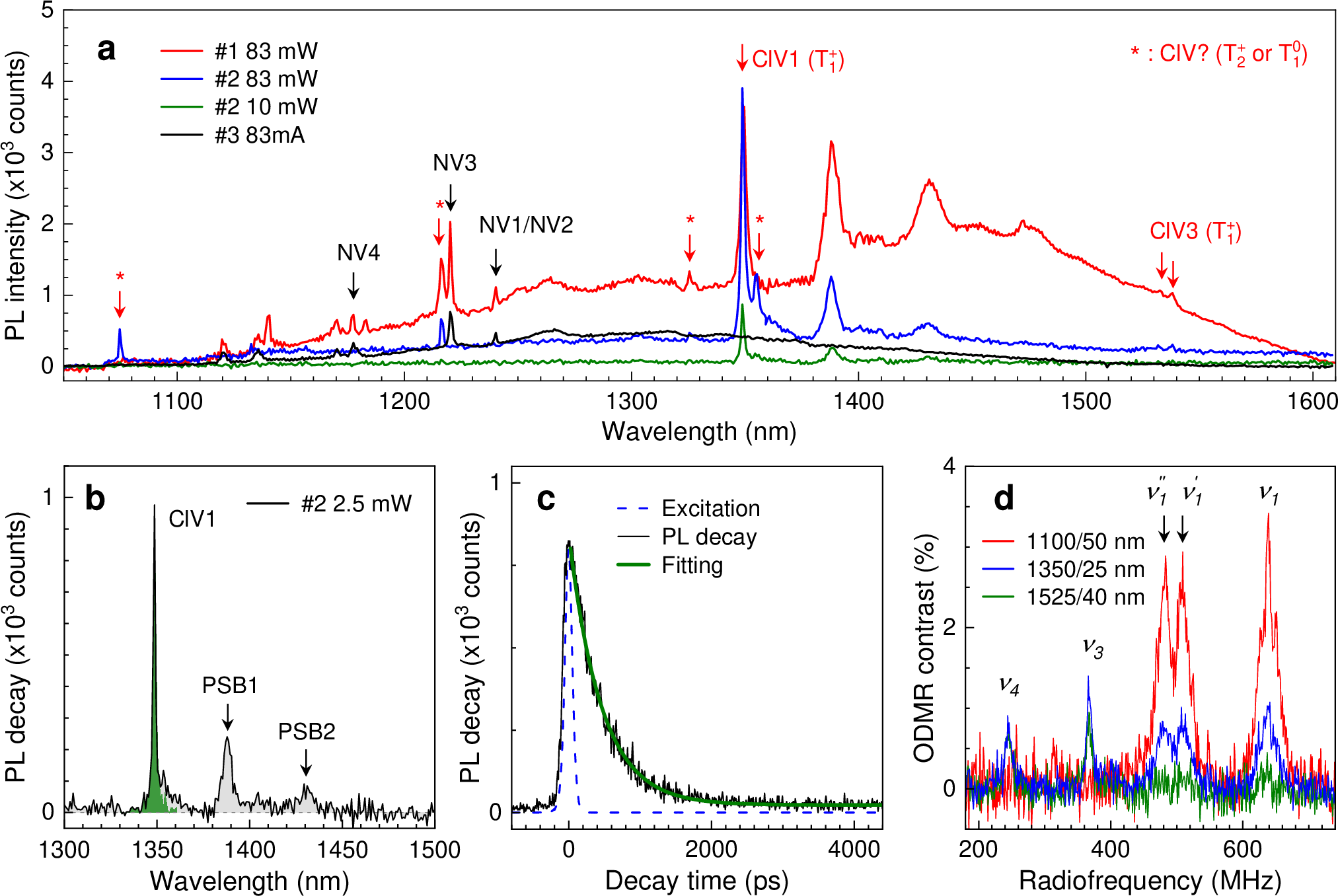
Figure 1: PL spectra and photoexcitation dynamics of Cl-related defects in 4H-SiC, revealing ZPLs spanning the O- and C-bands alongside leading PSBs and exceptional Debye-Waller factors.
Under low-power excitation, the highest PL intensity is associated with the ClV1 ZPL, ascribed to the on-axis configuration. The Debye-Waller factor reaches up to 39%, which is an order of magnitude larger than for NV centers in diamond and a significant improvement over SiC divacancy defects. The measured excited-state lifetime is remarkably short at 450 ps, potentially allowing GHz-rate photon emission, though nonradiative channels may contribute.
Importantly, at increased excitation powers, further ZPLs emerge, attributed to either alternate charge states or higher excited electronic levels of the Cl-related defects. Spectrally-resolved ODMR links these transitions to common spin-active species, confirming their multi-level structure and robustness.
Spin Structure and ODMR Signatures
Room-temperature operation of the Cl-related defects is secured by strong ground-state zero-field splitting (ZFS) in the sub-GHz range and robust hyperfine coupling to 35Cl nuclear spins. ODMR spectra present rich structure (Figure 2), including resolved hyperfine sidebands and secondary resonances, in contrast to non-spin-active controls and Ar-implanted samples.
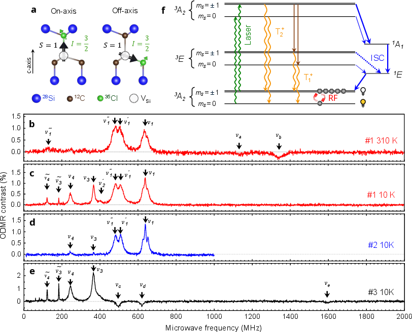
Figure 2: ODMR signals for different sample and temperature regimes, and schematic illustrating on-axis and off-axis ClV defect configurations and electronic spin coupling cycles.
Magnetic-field-dependent ODMR reveals complex splitting and mixing behaviors, captured by a spin Hamiltonian with parameters D=560 MHz, E=60 MHz, and hyperfine coupling A=−34 MHz for the dominant off-axis configuration (Figure 3). The observed transitions encode both electron and nuclear spin mixing, and simulation shows highly accurate correspondence to the measured field-evolution, supporting the underlying defect assignment.
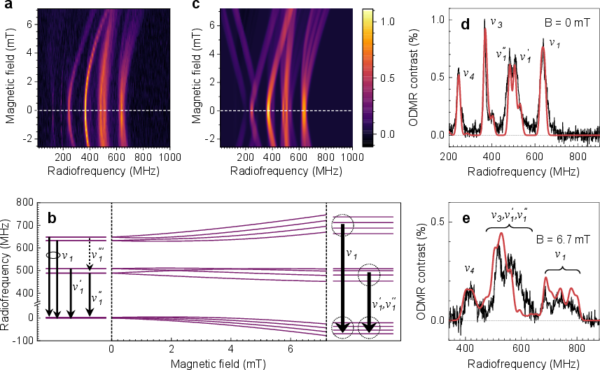
Figure 3: Experimental and simulated ODMR spectra as a function of external magnetic field, confirming hyperfine structure and zero-field splitting consistent with ClV defect models.
Coherent Spin Control and Quantum Memory Criteria
Coherent manipulation of the defect ground-state spin manifold is achieved with pulsed RF control protocols, including Ramsey interferometry and relaxation time measurements (Figure 4). The characteristic spin relaxation time T1 and inhomogeneous dephasing time T2∗ are both in the sub-microsecond regime (T1=660 ns, T2∗≃2 μs). While these times are below those of intrinsic vacancies and divacancies—where coherence can extend to ms timescales—the limit is attributed to charge-state conversions and metastability under optical excitation rather than intrinsic decoherence.
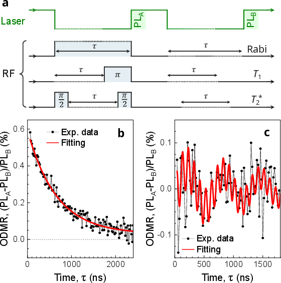
Figure 4: Pulse protocols and time-resolved measurements of spin lifetime and Ramsey fringes indicating coherent control and hyperfine-split precession.
The Ramsey experiment resolves closely spaced precession frequencies, confirming the strong hyperfine interaction and multi-level electronic-nuclear structure of the ClV system. These results establish all critical criteria for quantum memory functionality: spin initialization, coherent manipulation, and optically-detectable readout at telecom wavelengths.
Practical and Theoretical Implications
The experimental validation of Cl-related defects as coherent, telecom-band spin-photon interfaces unlocks several advantages for large-scale quantum networks:
- Integrated Photonics Compatibility: Wafer-scale SiC can be integrated with mature photonic platforms, facilitating device scaling and on-chip networking without external frequency converters.
- High-Debye–Waller Factor: Enhanced photon indistinguishability and collection efficiency can be expected compared to established defects.
- GHz-Scale Emission Rate: Short excited-state lifetimes promise fast, on-demand single-photon emission suitable for high-bandwidth networking.
- Room-Temperature Coherence: ODMR contrast and coherent control persist even at ambient conditions, favoring practical deployment.
Theoretical open questions include resolving detailed charge cycling mechanisms, configuration-dependent optical cycles, and strategies for stabilizing the spin-active charge state under resonant excitation—required for on-demand initialization and readout in device settings.
Future Directions
Immediate priorities include isolating single ClV emitters, optimizing nanofabrication for photonic cavity integration, and engineering the local charge environment to maximize T1 and 350. System-level work will explore nuclear spin-assisted quantum registers and telecommunication-band entanglement distribution. Comparative analysis with recent, independently observed Cl-related ODMR in SiC (Shafizadeh et al., 9 Feb 2026) will refine defect assignment and clarify multiplexing potential in heterogeneous device arrays.
Conclusion
Chlorine-related defects in 4H-SiC provide a viable, scalable, and fabrication-compatible platform for quantum memories operating natively at telecommunication wavelengths. Their simultaneous support for bright, indistinguishable emission and coherent ground-state spin control, combined with high Debye-Waller factors and robustness against temperature and magnetic field, position them as a premier defect class for the next phase of integrated quantum network development. Further progress in single-emitter control, photonic integration, and charge-state engineering is expected to fully establish their technological and foundational significance for quantum information science.

