- The paper demonstrates that optimizing reticle placement, particularly with Rotated and Contoured strategies, significantly enhances inter-wafer connectivity and overall network performance.
- It employs cycle-accurate modeling to reveal improvements of up to 250% in throughput and a 36% reduction in zero-load latency compared to baseline designs.
- The analysis shows reduced energy per byte and minimal router area overhead, making these strategies highly beneficial for scaling LLM and HPC systems.
Network Design Optimization for Wafer-Scale Systems Using Wafer-on-Wafer Hybrid Bonding
Introduction
The limitations of inter-chip communication bandwidth have become the principal bottleneck in scaling transformer-based LLM training, as communication bandwidth degrades significantly beyond chip boundaries. Wafer-scale integration (WSI), particularly through commercially accessible wafer-on-wafer (WoW) hybrid bonding, presents a vertical scaling alternative. In this paper, the authors systematically analyze how reticle placement within bonded wafers fundamentally dictates feasible interconnect topologies and, hence, end-to-end data movement efficiency. They characterize the topological impacts of four innovative reticle placement strategies—Aligned, Interleaved, Rotated, and Contoured—demonstrating their advantages through cycle-accurate modeling and design-space exploration. The work reveals substantial improvements in throughput, latency, and energy efficiency for LLM and high-performance computing (HPC) workloads enabled through sophisticated reticle-level network co-design.
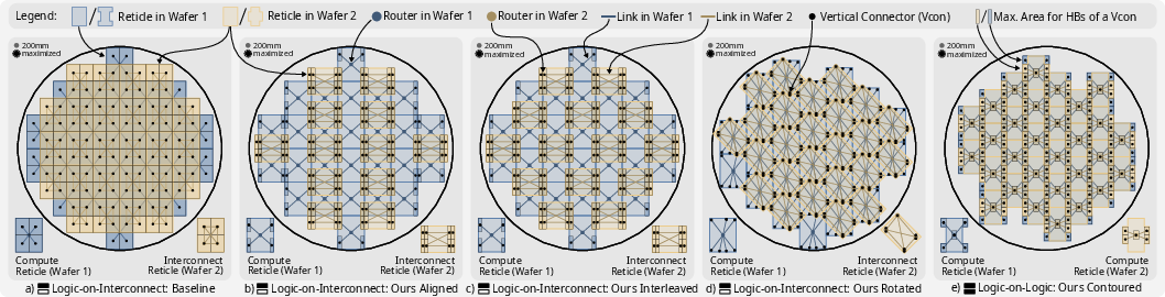
Figure 1: System visualizations of baseline and optimized reticle placements, highlighting the topological distinctions across Aligned, Interleaved, Rotated, and Contoured configurations.
Wafer-on-Wafer Hybrid Bonding Fundamentals
WoW hybrid bonding surpasses traditional chiplet-based WSI and reticle field stitching by delivering inter-wafer connections with sub-10 µm pitch, which eliminates the area and power overheads of PHYs required in die-to-die interfaces. Critically, only overlapping reticles on opposing wafers can be connected, so the network topology is constrained by the two-level 2D packing of reticles. For “logic-on-interconnect” architectures, only the top wafer hosts compute reticles while the bottom acts as a dense interconnect layer; in “logic-on-logic” architectures, both wafers integrate compute reticles, challenging the designer to maximize both compute density and communication connectivity under intense power and thermal budgets.
Topological Optimization via Reticle Placement
The paper formalizes the placement optimization problem: maximize the per-reticle radix (number of inter-wafer neighbors), thus minimizing average path length, under the process design rules and manufacturing constraints. The four proposed placements are:
- Aligned: Interconnect reticles are rotated and directly aligned with compute reticles, achieving up to six inter-wafer connections per interconnect reticle while keeping compute radix at four.
- Interleaved: Interconnect reticles are interleaved to form a distinct non-mesh connectivity, modestly increasing path diversity over the baseline.
- Rotated: Interconnect reticles are rotated by 45∘ and resized to maximize overlap, regularly enabling up to seven connections per reticle—the theoretical upper bound.
- Contoured: For dual-compute (logic-on-logic) wafers, contoured (H- and plus-shaped) reticles tessellate the wafer to enable five inter-wafer connections per reticle while maximizing silicon usage.
These physical arrangements yield topologies with higher connectivity and lower diameters compared to the conventional mesh, without violating reticle size, lithographic, or packaging constraints.
Detailed Experimental Results
Latency and Throughput
Cycle-accurate BookSim2 simulations under synthetic workloads (uniform, permutation, neighbor, tornado) and realistic Llama-7B training traces reveal significant latency and throughput advantages for optimized reticle placements.
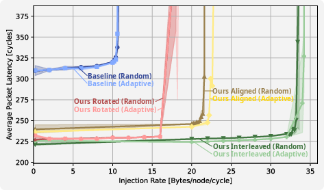
Figure 2: Latency vs. load for a 300 mm logic-on-interconnect system, showing improved saturation under optimized placements.
The Rotated placement, in particular, achieves up to a 250% improvement in saturation throughput and a 36% reduction in zero-load latency relative to the baseline, especially for permutation and uniform traffic—workloads emblematic of all-to-all communication in LLM training.
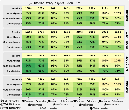
Figure 3: Throughput heatmap for logic-on-interconnect across various placements and traffic patterns.
Area, Power, and Energy
Router area overheads are minimal—buffer-dominated and vastly sublinear with respect to available reticle area for typical radix increases.
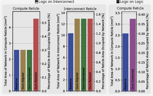
Figure 4: Router area analysis demonstrating negligible area impact of increased reticle radix due to buffer scaling.
At the network level, energy per byte is reduced by up to 38% for certain placements, with most gains attributable to reduced average hop count and more efficient utilization of high-bandwidth vertical links. Total network power at saturation can reach 4 kW, but this is compatible with the 15 kW wafer-level power envelope reported in prior large-scale AI accelerator implementations.
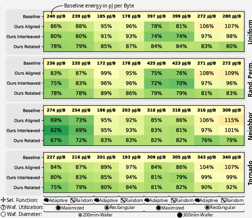
Figure 5: Network energy per byte heatmap for logic-on-interconnect, highlighting the efficiency of topological optimization.
Real-World Application Traces
On Llama-7B training workloads, latency reductions are even more pronounced due to the effect of path-length compression during load spikes and network congestion. The best placements reduce application-level average latency to 37% of the baseline.
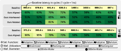
Figure 6: Trace-driven latency improvement for Llama-7B training scenarios, validating practical impact of co-designed reticle placement.
Implications and Future Prospects
This work redefines network scalability for monolithic silicon substrates by demonstrating that reticle placement is as critical as router microarchitecture or link bandwidth in wafer-scale communication efficiency. Optimal placement schemes allow for higher connectivity and broader bisectional bandwidths than mesh-derived baselines, triggering cascaded improvements in throughput, latency, and energy, with direct ramifications for LLM, MoE, and dense HPC workloads. The deployment of these techniques will require more advanced physical design automation that jointly optimizes routing, floorplanning, and manufacturing yield in the presence of hybrid bonding constraints.
Theoretically, maximizing per-reticle radix without violating reticle-mask limitations suggests continued topological innovation, particularly for nonregular packing, asymmetric reticle design, and multi-wafer (beyond two) vertical stacks. Practically, enabling logic-on-logic architectures and advanced cooling (e.g., through silicon vias or microfluidics) compounds the gains, while continued improvements in hybrid bonding pitch and wafer utilization will push the boundary of monolithic system integration for AI and HPC.
Conclusion
Through comprehensive exploration and cycle-accurate evaluation, this study establishes that the achievable on-wafer network topology in wafer-scale integration is fundamentally dictated by reticle placement across bonded wafers. The proposed placement strategies—especially Rotated and Contoured—yield substantial improvements in throughput, latency, and energy efficiency, directly benefiting demanding communication-bound workloads such as LLM training. This result signals reticle placement optimization as a key driver in the continued vertical scaling of AI accelerators and supercomputers.