- The paper demonstrates high-fidelity (over 99.9%) single-electron shuttling and junction routing using only eight atomic voltage pulses and eleven control channels.
- Its innovative T-junction design integrates 54 quantum dots with robust voltage multiplexing, enabling deterministic multi-electron pattern control and SWAP operations.
- Results show that ultra-low error rates from repeated charge looping support scalability for 2D spin qubit architectures in quantum error corrected systems.
Conveyor-Mode Electron Shuttling through a Si/SiGe T-Junction: Architectures, Fidelity, and Implications for Scalable Spin Qubits
Introduction
The realization of robust two-dimensional (2D) qubit architectures is essential for surface-code quantum error correction and large-scale quantum computation using semiconductor qubits. Existing scalability in silicon spin qubit platforms is limited by linear geometries, wiring bottlenecks, and the challenge of dynamic qubit routing. Conveyor-mode electron shuttling has emerged as a highly scalable approach for charge and spin transport, requiring minimal control lines independent of shuttle distance. However, a demonstration of 2D charge routing—including junction operation with charge pattern control—has thus far remained elusive. This study presents a silicon/silicon-germanium (Si/SiGe) quantum dot (QD) device that implements conveyor-mode shuttling over a 54-dot T-junction, enabling high-fidelity routing of single and multiple electrons using only eight atomic voltage pulses and eleven control channels (2601.03942).
Device Architecture and Pulse Protocols
The fabricated T-junction device integrates two orthogonal, independently pulsed shuttle lanes (x- and y-shuttle), interconnected at a 90° junction. The electron potential landscape is defined by three overlapping gate layers, with 218 gates grouped into eight periodic sets, enabling robust voltage multiplexing.
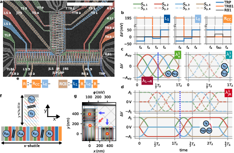
Figure 1: False-color SEM of the device and schematic representation of atomic pulses, with simulation of electron probability densities during routing through the T-junction.
Key device specifications:
- Shuttle lanes: Each lane hosts QDs under every fourth gate (280 nm pitch, total of 54 QDs).
- Control reduction: All transport and routing is accomplished with only eight atomic pulses and eleven terminals (including initialization/readout).
- Conveyor-mode operation: Forward shuttling in each lane is effected by phase-locked sinusoidal gate modulation; T-junction transfer uses coordinated reversal and halting to effect continuous state transfer.
- Simulation: Electrostatic and wavefunction modeling shows adiabatic transfer with orbital splitting evaluated throughout the junction.
Deterministic Single Electron Shuttling and Routing
Shuttling is validated by initializing a single electron at one device end and sequentially transporting it through the junction, as confirmed by proximal charge sensing at device terminals.
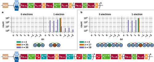
Figure 2: Applied pulse protocols and histograms for charge detection after shuttle operations, showing unambiguous transport and absence of charge for reference sequences.
High-fidelity transport (F>99.9%) is maintained for both long-range linear shuttling (up to 35 dots) and junction routing at instantaneous velocities of 270 mm/s. Error analysis reveals that transport fidelity is limited primarily by initialization/readout (SPAM) rather than shuttle dynamics; infidelities are undetectable within the measurement statistics set by total repetition counts.
Tuning Parameter Space and Charge Looping
Junction performance is mapped over a broad range of drive amplitudes (AJ) and velocities (vJ), revealing minimal dependence of fidelity on amplitude above a sharp threshold (AJ≳133 mV). To measure ultra-low shuttle infidelities, single charges are looped up to 106 times around the T-junction, amplifying rare error events.
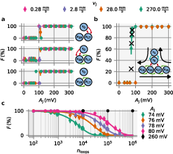
Figure 3: Junction transfer parameter sweeps and results of charge looping, illustrating per-loop fidelities and statistical error accumulation.
The extracted per-loop fidelity for junction transfer, at optimal parameters, is F1=99.9999999−0.0000009+0.0000000—no measurable errors across 106 repetitions. The shuttle operation shows statistical independence; accumulation of infidelity is consistent with the prediction Ftotal(nloops)=F1nloops.
Multi-Electron and Pattern Control
Patterned initialization and co-shuttling of up to 54 electrons is demonstrated. Electron configurations are arbitrarily loaded into both shuttle lanes; routing and pattern SWAP operations are performed by sequenced atomic pulses.
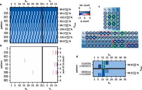
Figure 4: Simultaneous control and transport of periodic occupancy patterns; schematic and experimental realization of the SWAP operation by conveyor-mode transfer in the T-junction.
Pattern fidelities reach Ftotal≈99%, with deviations attributed to SPAM-induced double occupancy—no evidence of unintentional interdot tunneling or charge loss aside from expected edge effects.
A native exchange of two patterns is realized by sequenced conveyor operations, emulating a SWAP gate at the charge level with Ftotal≥99.8%. This operation is of particular relevance for qubit routing in error-corrected architectures, as it replaces exchange-based gates with physically deterministic position interchange.
This work demonstrates that complex quantum dot intersections—with more than 50 QDs—can be controlled using a minimal set of voltage lines and highly repeatable atomic pulse sequences. The high fidelity, low complexity, and robustness of the conveyor-mode T-junction directly address the principal barriers to scalable spin-based quantum information processors:
- Wire count minimization: The entire 2D routing operation is performed with eight atomic pulses, enabling dense interconnects free from local wiring congestion.
- Error correction viability: The observed per-operation error rates are well below the thresholds for surface code error correction, even under accelerated error accrual via 106-fold repetition.
- Classical/quantum co-integration: The low drive and readout complexity is compatible with monolithic integration of classical electronics with quantum dot planes, facilitating scalable layered architectures.
- Qubit exchange and routing: Deterministic pattern SWAP without spin exchange provides a native mechanism for logically permuting qubit registers, reducing reliance on complex pulse-level control and improving device tolerance to disorder.
Conclusion
This study establishes conveyor-mode T-junctions as a viable mechanism for high-fidelity, low-complexity, and highly scalable charge and spin transport in 2D silicon quantum dot arrays. The demonstrated fidelities and robust pattern control pave the way toward practical quantum error correction using shuttling-based architectures, with direct applicability to future integrated quantum-classical systems. Future work will focus on the direct demonstration of spin-coherent transfer through junctions, improved disorder tolerance, and integration with error-corrected logical operations (2601.03942).

