An integrated photonic millimeter-wave receiver with sub-ambient noise
Abstract: Decades of progress in radiofrequency (RF) transistors and receiver frontends have profoundly impacted wireless communications, remote sensing, navigation, and instrumentation. Growing demands for data throughput in 6G networks, timing precision in positioning systems, and resolution in atmospheric sensing and automotive radar have pushed receiver frontends into the millimeter-wave (mmW) and sub-mmW/THz regimes. At these frequencies, however, the noise performance of field-effect transistors (FETs) degrades rapidly due to parasitic effects, limited carrier mobility, hot electrons, and shot noise. Parametric transducers that couple electromagnetic signals to optical fields offer quantum-limited sensitivity at room temperature. Electro-optic materials enable receivers that convert RF signals into optical phase shifts. While early demonstrations used resonant devices and recent efforts have focused on cryogenic microwave-to-optical quantum transduction, room-temperature electro-optic receivers have yet to achieve noise figures comparable to their electronic counterparts. Here we demonstrate a room-temperature integrated cavity electro-optic mmW receiver on a lithium tantalate (LiTaO3) photonic integrated circuit with 2.5% on-chip photon-number transduction efficiency, achieving 250 K noise temperature at 59.33 GHz--matching state-of-the-art LNAs. We report the first direct resolution of thermal noise in cavity electro-optic transduction, showing the system is fundamentally limited by thermal photon occupation (~100) in the mmW cavity. Our work establishes integrated photonics as a path to surpass electronic LNAs while offering exceptional resilience to strong electromagnetic inputs and immunity to EMI, establishing cavity electro-optics as a low-noise, chip-scale, EMI-resilient receiver frontend for mmW applications and scalable analog processing in the optical domain.
Paper Prompts
Sign up for free to create and run prompts on this paper using GPT-5.
Top Community Prompts
Explain it Like I'm 14
Overview
This paper explains how to build a tiny, chip-based receiver that can “listen” to millimeter-wave signals (very high-frequency radio waves, like those used in advanced wireless systems) by turning them into light inside a photonic circuit. The big deal: it can do this at room temperature with less noise than what the surrounding air would normally cause (sub-ambient noise), which is unusually good for radio receivers.
Key Objectives and Questions
The researchers set out to:
- Make a compact device that converts weak millimeter-wave signals into optical signals reliably and with very low added noise.
- Choose and control the physical processes so that the “quiet” conversion path dominates and the “noisy” one is suppressed.
- Design and tune a microwave resonator (the part that stores the radio-wave energy) to work efficiently at both 30 GHz and 60 GHz on the same chip.
- Understand and measure where the device stays linear (accurate) and where it starts saturating (compressing), so it can handle strong signals safely.
- Compare this photonic receiver’s performance to the best electronic amplifiers and other optical/atomic methods.
Methods and Approach (in everyday terms)
Think of the device as two “tuning forks” that talk to each other: one vibrates with radio waves (microwave cavity) and the other with light (optical cavity). A steady laser “pump” shines into the optical cavity. Because of a special property of the material (the electro-optic or “Pockels” effect), the radio-wave vibrations can slightly change the light’s frequency, creating tiny “side tones” of light.
- Stokes and anti-Stokes: When you shake light with a radio wave, you can get two kinds of side tones. One slightly lower in frequency (Stokes), and one slightly higher (anti-Stokes). The anti-Stokes path is the clean, coherent way to convert radio to light. The Stokes path can add extra quantum noise (like creating unwanted pairs of photons).
- The trick: The team designed coupled optical rings to suppress the Stokes side, making the anti-Stokes side the main highway for conversion. That keeps the converted light cleaner.
- Resonance and coupling: Resonance is like pushing a swing at the right rhythm. The optical and microwave cavities are tuned so energy transfers efficiently. “Critical coupling” means energy flows in and out just right; “overcoupling” means you intentionally let energy leak faster to reduce the effect of thermal noise (heat-generated “jiggle”).
- Heterodyne detection: After converting radio to light, they measure the light by mixing it with another laser to make a beat note. This is like tuning your ear to the difference between two pitches, which lets them read out the radio signal precisely.
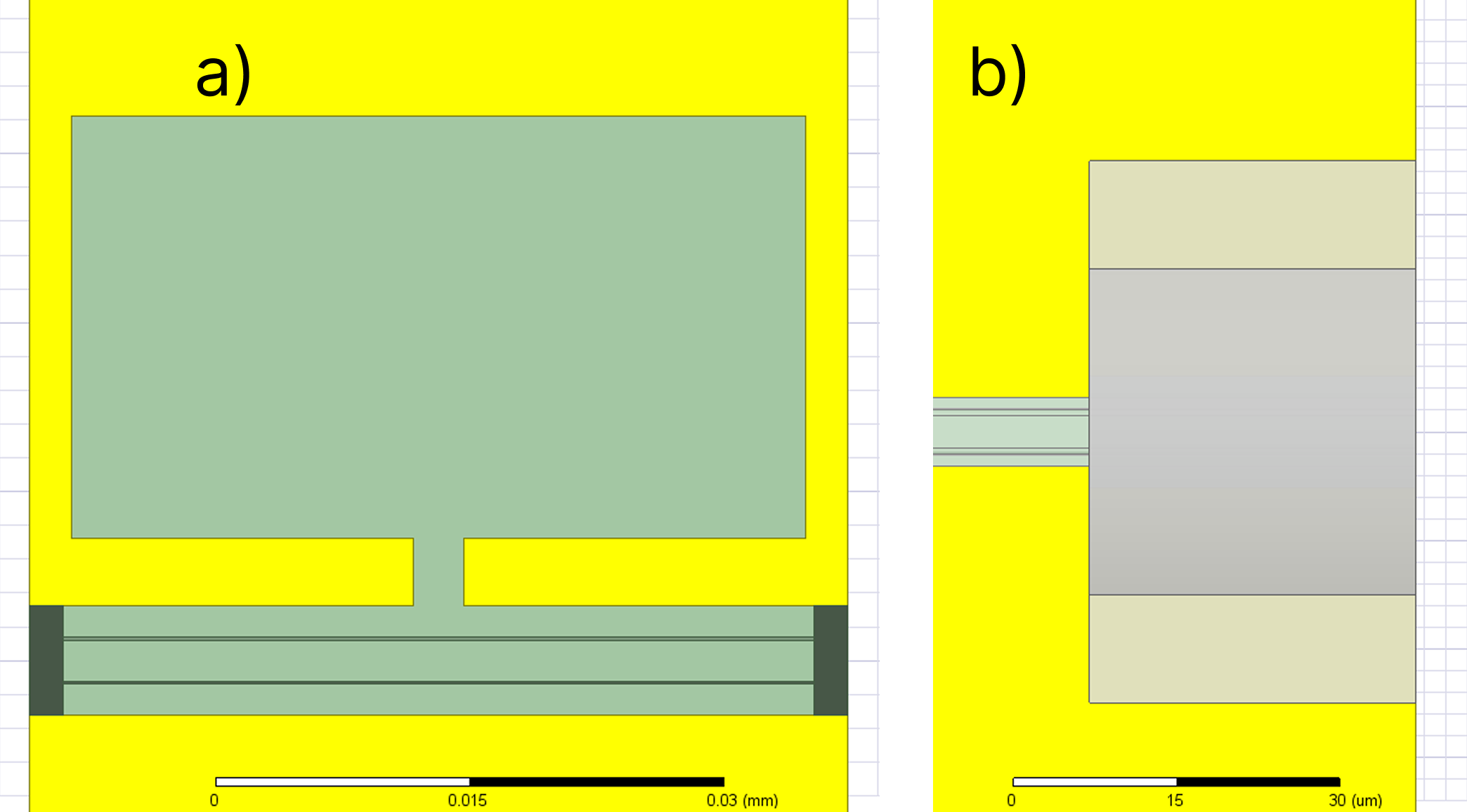
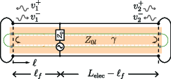
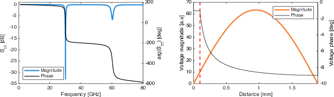
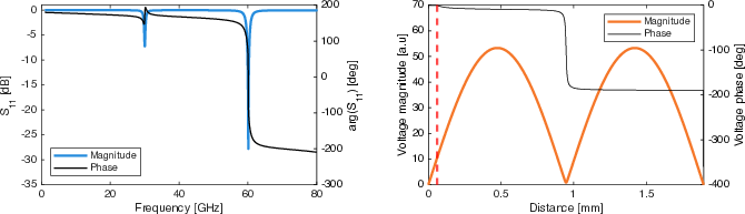
- Microwave resonator design: They built a coplanar waveguide (CPW) resonator with periodic “T-cells” and shorted ends (airbridges). These features slow down and strengthen the microwave field where it matters, reduce loss, and let them place the measurement probe at different points to hit the right coupling for 30 GHz and 60 GHz.
- How strong is the coupling? A key number called tells how strongly radio waves and light interact in the chip. They calculate it from how well the fields overlap in 3D and how effectively the electrodes and waveguides concentrate the electric field in the optical waveguide.
Main Findings and Why They Matter
- Clean, bidirectional conversion: By favoring the anti-Stokes process, the device converts radio waves to light (and vice versa) coherently. In the practical, low-coupling regime, conversion efficiency scales linearly with a quantity called “cooperativity” (how strongly the two cavities talk).
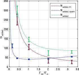
- Sub-ambient noise at room temperature: The device’s total added noise comes from two sources:
- Quantum noise (shot noise of light), which goes down as conversion efficiency goes up.
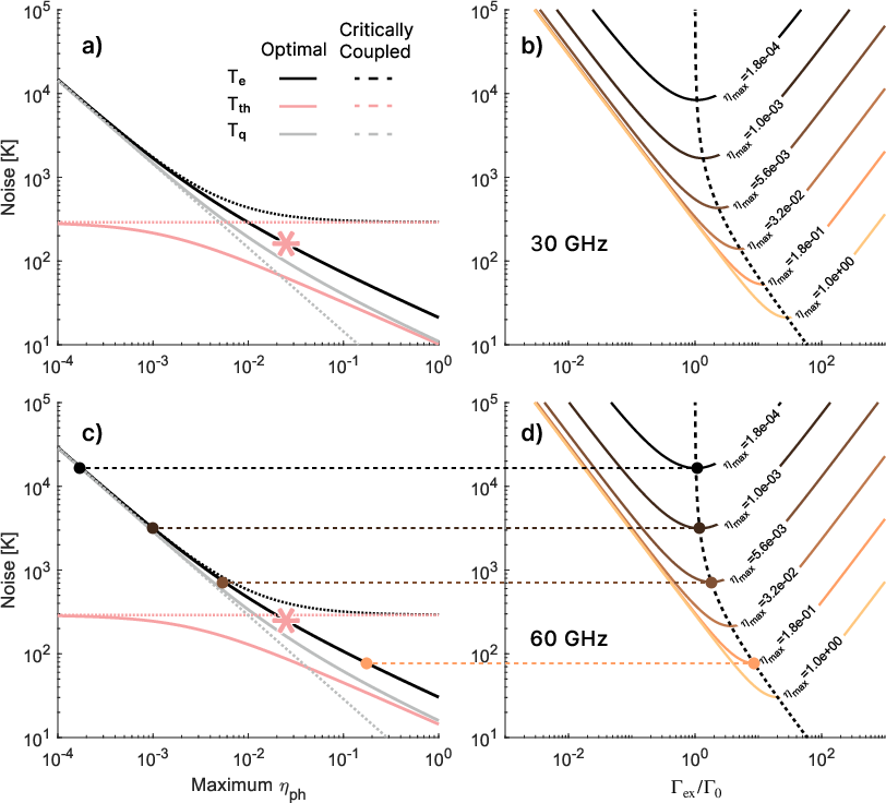
- Thermal noise (from the microwave cavity’s “hot” environment), which can be reduced by overcoupling the microwave resonator so heat leaks out to the measurement port rather than into the device.
- By balancing these, they show the receiver’s effective noise can be below what a standard electronic amplifier at room temperature would add, and even below the “ambient” thermal limit.
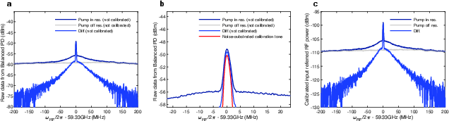
- Tunable coupling for optimal noise: They measured and modeled how the receiver’s added noise changes when they move the probe along the microwave resonator to adjust the external coupling rate. Near critical coupling, the quantum noise contribution is minimized. With proper overcoupling, the thermal part drops, allowing noise figures below 3 dB in favorable cases.
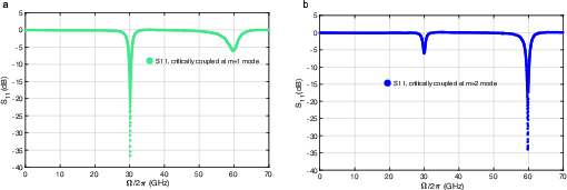
- Works at multiple bands: The same resonator can be fed at different points to critically couple either the 30 GHz mode (m=1) or the 60 GHz mode (m=2). Measurements of reflection () confirm this. The field shapes for both modes are well matched to the optical rings, giving strong interaction.
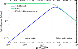
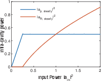
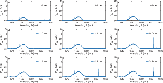
- High-power behavior is safe and predictable: As input power grows, the system first converts more efficiently, then hits a “compression point” (IP1dB) where conversion starts to saturate because the optical pump inside the cavity is depleted. Past that, the device naturally shifts into forming an electro-optic frequency comb (a set of evenly spaced optical lines), which spreads energy and helps prevent damage. This makes the receiver robust against sudden strong signals or interference.
Why it’s important: Electronic low-noise amplifiers (LNAs) are great, but at millimeter-wave frequencies they often need cryogenic cooling for the very lowest noise. This chip can achieve very low noise at room temperature by using light to measure radio, potentially beating or complementing LNAs without bulky cooling.
Implications and Potential Impact
- Better wireless and radar: A quieter, room-temperature millimeter-wave receiver could boost sensitivity in 5G/6G backhaul, automotive radar, and remote sensing.
- Radio-over-fiber: Converting radio directly to light on-chip makes it easier to send signals over long distances in optical fiber with minimal added noise.
- Energy-efficient sensing: Avoiding cryogenic amplifiers saves power and complexity, making systems smaller and greener.
- Quantum and hybrid systems: Clean, coherent radio-to-light conversion is useful for connecting microwave devices (like superconducting circuits) to optical networks in future quantum technologies.
- Robust operation: The built-in handling of high-power signals and the move into comb formation means the device is resilient to electromagnetic interference and overloads, which is practical in real-world environments.
In short, this work shows a new way to receive and process very high-frequency radio signals using light, on a chip, with exceptionally low noise at room temperature. That opens doors to faster, more sensitive, and more compact communication and sensing systems.
Knowledge Gaps
Knowledge gaps, limitations, and open questions
Below is a focused list of what remains missing, uncertain, or unexplored, formulated to be concrete and actionable for future research.
- Quantify the residual Stokes-channel leakage when using coupled rings for suppression: measure the Stokes suppression ratio, its impact on added noise via two-mode squeezing, and the corresponding trade-off with anti-Stokes conversion efficiency.
- Analyze performance under realistic dispersion mismatch (nonzero δs, δas): provide tolerance budgets for phase mismatch between optical FSR and microwave resonance, and demonstrate active compensation strategies (e.g., thermal tuning or microheaters).
- Correct and validate the thermal occupation used in noise derivations: the SI defines n_th = ℏΩ/k_BT (inverted); re-derive added-noise and noise-figure expressions with n_th = k_BT/(ℏΩ) and reassess all reported “sub-ambient” claims under the corrected model.
- Include non-ideal detection-chain noise in the input-referred noise model: quantify the contributions from LO relative-intensity/phase noise, finite photodiode quantum efficiency, electronic baseband amplifier noise, and imperfect balancing in heterodyne detection.
- Provide measured conversion bandwidth and its dependence on pump power, detuning, and coupling rates: validate the reversed-dissipation assumption (Γ ≫ κ) experimentally and quantify S(Δ) over frequency.
- Characterize dynamic range beyond the simulated IP1dB: measure IP1dB on-device, intermodulation distortion (IIP3), spurious-free dynamic range (SFDR), and multi-tone behavior, especially near the onset of EO comb formation.
- Model and measure transient response and stability under time-varying inputs: quantify settling times, ringing, and bandwidth-dependent gain variations, including the effect of pump and microwave detuning noise.
- Co-optimize optical coupling (γo) together with microwave coupling (γe): extend the overcoupling optimization to include γo and pump power to jointly minimize total noise temperature while maximizing conversion efficiency.
- Incorporate external feedline thermal noise into the noise-temperature model: account for thermal noise from the source at room temperature and its weighting with internal and external coupling, not only Γ0/Γex.
- Assess radiative cooling limits in practical packaging: quantify how probe, contact transitions, and housing alter Γex, internal loss, and the ability to reduce effective thermal noise below ambient.
- Experimentally extract g0 and validate its scaling: measure g0 across 30–60 GHz (and higher) to verify the predicted g0 ∝ √Ω (or ∝ Ω under length scaling), including the role of racetrack length L, overlap ξ, and electrode geometry.
- Evaluate electro-optic material effects under realistic operating conditions: quantify photorefractive and photothermal drift in LiTaO3, pump-induced refractive index changes, and long-term stability under high optical/microwave powers.
- Demonstrate frequency-locking and resonance-stabilization schemes: detail servo strategies to maintain triple resonance and assess their impact on conversion stability, added noise, and long-term drift.
- Explore higher-order harmonic operation (m > 2): determine phase-matching limits, overlap integral degradation, and conversion efficiency trends for W-band and beyond.
- Perform fabrication tolerance and yield analysis: quantify sensitivity of T-cell periodicity, racetrack length, electrode alignment, and airbridge shorts to performance metrics (Qm, g0, ξ, Γex, κ) and report device-to-device variability.
- Characterize maximum power handling and thermal limits: measure heating, optical damage thresholds, and mm-wave electrode reliability under sustained high input power; assess how thermal load alters NF and η.
- Develop practical coupling solutions beyond movable probe landing: design integrated 50 Ω terminations, tunable couplers/matching networks, or antenna interfaces suitable for packaged systems and quantify the resulting S11 and Γex control.
- Standardize noise-figure benchmarking across platforms: specify bandwidth, frequency, temperature, detection scheme, and calibration methods to enable apples-to-apples comparisons with LNAs, Rydberg receivers, and other photonic systems.
- Quantify upconverted spurious content and spectral purity: measure sideband-phase noise, adjacent-channel leakage, and comb-induced spurs versus input power, and provide mitigation strategies for communication/radar use cases.
- Report environmental sensitivity and temperature dependence: characterize NF, η, and Q factors versus ambient temperature, mechanical vibration, and EMI; document the operating window where “sub-ambient” noise is maintained.
- Detail the calibration procedure for “on-chip input-referred quantum noise” and ηcrit: provide measurement uncertainty, traceability, and repeatability across devices; reconcile the low ηcrit = 2.5% with claimed quantum-limited operation.
- Validate Γ ≫ κ across operating bands and power levels: supply measured Γ, κ, and their scaling with frequency and input power to substantiate adiabatic elimination and bandwidth claims.
- Model multimode and backscattering effects in the optical racetrack: quantify mode splitting, counter-propagating coupling, and their influence on anti-Stokes transduction, residual Stokes noise, and stability under pump detuning.
- Include photodiode and downstream electronics nonlinearity in system linearity analysis: determine if detection-chain saturation, clipping, or compression materially limits the overall receiver IP1dB and SFDR.
Practical Applications
Immediate Applications
Below are practical, deployable applications that leverage the paper’s integrated photonic millimeter-wave receiver, its design methods (triply resonant cavity electro-optics, anti-Stokes suppression, overcoupled microwave resonators), and its noise optimization (sub-ambient noise via radiative cooling and quantum-limited optical readout).
- Healthcare, environmental monitoring, and atmospheric science: compact room‑temperature 60 GHz oxygen radiometers for weather and air-quality sensing
- What: Use the receiver’s sub-ambient input-referred noise and optical readout to build portable, fiber-fed radiometers operating near the oxygen absorption line (~60 GHz).
- Why now: The device’s reversed-dissipation regime (Γ >> κ) and overcoupling strategy allow noise figures below physical temperature without cryogenics.
- Tools/products/workflows: Fiber-coupled photonic mmWave radiometer modules; workflow includes setting microwave external coupling via probe landing position to minimize total noise (using Γ0/Γex optimization), anti-Stokes-only transduction to suppress added squeezing noise, and balanced heterodyne optical detection.
- Assumptions/dependencies: Stable optical pump laser and heterodyne LO; robust packaging to keep cavity detuning fixed; sufficient conversion efficiency (ηcrit ≈ few percent reported) balanced by overcoupling to cool thermal noise; bandwidth set by optical linewidth.
- Telecommunications (radio-over-fiber, fronthaul/backhaul) for 5G/early 6G FR2 bands (28–39 GHz) and pilot E‑band deployments (70–86 GHz)
- What: Deploy photonic remote antenna units (RAUs) that transduce mmWave RF to optical and send it over fiber to centralized processing, replacing or complementing LNAs in noisy or constrained sites.
- Why now: Demonstrated operation at 30/60 GHz and multi-band capability via resonator harmonics; the receiver’s EMI resilience (saturation without damage past IP1dB) suits urban installations.
- Tools/products/workflows: Photonic RF front‑end modules with CPW–T‑cell resonators and coupled optical rings; workflows include unit-cell ABCD design to set resonances, landing-position tuning for critical or over-coupling, and optical heterodyne digitization at the hub.
- Assumptions/dependencies: Integration with existing ROF infrastructure; laser stabilization; packaging to manage temperature drift; current η in the few-percent range implies system-level gain planning.
- Defense and industrial monitoring: EMI-hardened mmWave receivers for hostile or electrically noisy environments
- What: Field sensors that withstand high instantaneous RF (IP1dB saturation rather than failure), transduce to optical, and carry data over fiber immune to EMI.
- Why now: The paper’s pump-depletion physics and EO comb onset indicate graceful saturation; optical readout via fiber reduces susceptibility to electromagnetic interference.
- Tools/products/workflows: Ruggedized fiber-fed mmWave field probes; operating recipe includes operating in anti-Stokes branch, setting Γex to minimize noise, and calibrating added noise via optical shot-noise and thermal occupancy.
- Assumptions/dependencies: Mechanical robustness; environmental control to keep resonances aligned; appropriate sector certification.
- Automotive and security imaging pilots: fiber-distributed mmWave sensing nodes for short-range imaging and radar prototyping
- What: Deploy photonic receivers in early-stage 77–81 GHz radar prototyping and security screening pilots, with optical transport to centralized processing.
- Why now: Multi-harmonic operation (m=1,2 demonstrated at 30/60 GHz) and g0 scaling with frequency provide a path to higher bands; photonic RAUs reduce front-end weight and EMI sensitivity.
- Tools/products/workflows: Compact photonic sensing nodes and fiber aggregation; workflows replicate the device’s landing-position coupling tuning and noise-optimal overcoupling.
- Assumptions/dependencies: Frequency scaling of materials and electrodes; packaging for higher conductor losses; optical linewidth limits bandwidth, so application should match sensor’s effective BW.
- Academic and industrial design acceleration: semi-analytical CPW resonator layout method and transduction/noise optimization framework
- What: Immediate use of the paper’s unit-cell ABCD matrix approach to quickly design periodic CPW resonators with T-cells; use the derived noise/η formulas to pick optimal Γ0/Γex.
- Why now: The workflow reduces FEM sweeps and speeds iteration; noise expressions directly link ηmax, coupling ratio, and added noise temperature/NF.
- Tools/products/workflows: CAD kits and scripts that extract unit-cell S-parameters, compute phase constants, set resonator length, scale to target frequency, and select landing positions for critical coupling; lab workflows to calibrate noise via optical heterodyne and thermal occupation.
- Assumptions/dependencies: Access to FEM tools (e.g., HFSS), established LiTaO3 or TFLN process; training on photonic–microwave co-design.
- Test and measurement: optical mmWave spectrum/power analyzer for labs
- What: A fiber-coupled optical readout front‑end to measure mmWave power spectra without cryogenic LNAs, exploiting the photonic receiver’s low added noise.
- Why now: The input-referred quantum noise can be calibrated via ηcrit and heterodyne shot-noise; radiative cooling reduces thermal noise.
- Tools/products/workflows: Modular photonic mmWave receiver heads with optical outputs to lab photonic digitizers; procedures for detuning control, anti-Stokes-only operation, and NF calibration.
- Assumptions/dependencies: Stable laser and LO; known system insertion loss to refer measurements to the DUT; conversion efficiency remains modest—compensate with optical gain stages.
Long-Term Applications
Below are applications that are compelling but require further research, scaling in conversion efficiency/cooperativity, broader frequency coverage, packaging maturity, and/or ecosystem integration.
- Telecommunications (mass 6G deployment): LNA-free or hybrid photonic RAUs across FR2/E/V bands with standardized ROF interfaces
- What: Large-scale replacement or augmentation of electronic LNAs with photonic receivers for distributed MIMO, beamforming, and ultra-dense small cells.
- Why it needs R&D: Requires higher cooperativity (C), improved g0 (lower VπL and stronger field overlap), wider effective bandwidth (beyond optical linewidth constraints), and robust packaging/temperature compensation.
- Potential products/workflows: Standardized photonic RF front-end modules; automated Γex tuning and self-calibrating noise optimization; integrated lasers and balanced detectors on chip.
- Assumptions/dependencies: Supply chains for LiTaO3/TFLN; reliability under outdoor conditions; regulatory approvals for fiber-fed RF front-ends.
- Automotive radar and advanced sensing: production-grade 77–81 GHz photonic receivers and fiber-distributed radar arrays
- What: Fiber-fed phased radar arrays with photonic front-ends, enabling centralized processing and simplified radome electronics.
- Why it needs R&D: Frequency scaling to W-band with acceptable conductor losses; integrated multi-channel arrays; system-level calibration and stability across temperature and vibration.
- Potential tools/products: Multi-beam photonic radar modules; EO comb-based mmWave LO distribution; integrated packaging co-designed for automotive standards.
- Assumptions/dependencies: Increased g0 at higher Ω (leveraging length scaling where g0 ∝ Ω); reliable anti-Stokes suppression across channels; manufacturing yield.
- Space and satellite communications: Ka/V-band photonic receivers for payloads and ground stations without cryogenics
- What: Lightweight, power-efficient, room-temperature low-noise receivers, with optical fiber or free-space optical backhaul.
- Why it needs R&D: Radiation-hard photonic materials and electrodes, thermal/vacuum robustness, broader frequency coverage, and rugged lasers/photodiodes.
- Potential products/workflows: Space-rated photonic RF front-ends; optical fronthaul linking phased arrays to centralized processors; EO comb sources for frequency synthesis.
- Assumptions/dependencies: Materials resilience; precise thermal control; long-lifetime optical sources.
- Radio astronomy and scientific radiometry: large arrays of room-temperature photonic mmWave receivers
- What: Replace or complement cryogenic LNAs in array receivers where fiber simplifies distribution and sub-ambient NF improves sensitivity at room temperature.
- Why it needs R&D: Scaling conversion efficiency, reducing optical insertion loss, and controlling cavity detuning across large arrays; expanded frequency range.
- Potential tools/products: Array-grade photonic receiver tiles; optical calibration injection; centralized optical DSP backends.
- Assumptions/dependencies: Stable lasers for many elements; per-element Γex optimization; comprehensive calibration workflows.
- Quantum networking interfaces (microwave–optical transduction)
- What: Use bidirectional, beam-splitter-type anti-Stokes conversion to link cryogenic microwave qubits or sensors to low-loss optical channels.
- Why it needs R&D: Moving from room temperature mmWave to cryogenic and lower‑frequency regimes with higher cooperativity; ultra-low-added-noise operation at the quantum limit; integration with superconducting platforms.
- Potential tools/products: On‑chip microwave‑optical transducers co‑packaged with qubits; cryo-compatible photonic packaging.
- Assumptions/dependencies: Material and design adaptations for cryo; suppression of Stokes-induced squeezing noise; compatibility with quantum error budgets.
- Photonic mmWave synthesizers and signal generation via EO comb formation
- What: Exploit pump depletion and EO comb formation beyond IP1dB to build coherent mmWave sources and frequency-multiplexed transceivers.
- Why it needs R&D: Controlled, efficient comb dynamics; phase coherence; integrated feedback for spectral shaping; robust high-power operation.
- Potential tools/products: EO comb-based LO modules; multi-tone transceivers; photonic frequency converters.
- Assumptions/dependencies: Stable high-power optical pumps; precise dispersion control; thermal management of electrodes and waveguides.
- Policy and infrastructure impacts: greener RF infrastructure via cryogen-free receivers and fiber-distributed front-ends
- What: National infrastructure upgrades prioritizing energy-efficient, EMI-resilient, fiber-linked RAUs with reduced maintenance.
- Why it needs R&D: Cost/benefit validation at scale, interoperability standards, and workforce training in photonic–RF co-design.
- Potential tools/workflows: Standardized photonic RAU specifications; certification frameworks; deployment playbooks for telecom operators.
- Assumptions/dependencies: Market acceptance; standardization bodies engagement; lifecycle reliability data.
Notes on cross-cutting assumptions and dependencies:
- Device physics: Current demonstrations operate in the reversed-dissipation regime; the effective bandwidth is set by the optical linewidth. Anti-Stokes-only operation (via coupled rings) is important to minimize added squeezing noise.
- Noise optimization: Sub-ambient noise hinges on microwave overcoupling (Γ0/Γex < 1) to radiatively cool the thermal bath and on calibrated optical shot-noise readout; conversion efficiency η remains a critical lever.
- Materials and packaging: High‑Q optical cavities in LiTaO3/TFLN with low microwave loss electrodes; temperature stabilization and detuning control are essential for field deployment.
- System integration: Stable optical pumps/LOs, balanced detectors, and fiber plant integration are required; landing-position tuning is a practical knob for Γex but should be replaced by designed coupling networks in products.
Glossary
- ABCD matrix: A 2×2 transfer matrix used to model and cascade linear two-port networks, such as periodic transmission-line unit cells. "characterize each unit cell by the transfer (ABCD) matrix"
- adiabatically eliminated: An approximation where a fast, highly damped mode is removed from the dynamics, leaving an effective description for the slower modes. "the microwave mode can be adiabatically eliminated"
- airbridge short-circuits: Metal bridges that short CPW ground planes across the signal line to enforce boundary conditions like shorts at line ends. "the reflected phase from the airbridge short-circuits"
- antiâStokes process: The upconversion process where a photon gains energy (frequency increases) by absorbing a quantum from a lower-frequency field (e.g., microwave). "the antiâStokes process, as the coherent transduction channel, is our preferred mechanism."
- balanced detection: An optical detection technique that subtracts currents from two photodiodes to reject common-mode noise (e.g., LO noise). "and splitting the beam for balanced detection."
- beam-splitter process: A light–matter interaction described by a Hamiltonian that swaps excitations between two modes, enabling coherent conversion. "one is the beam-splitter process with anti-Stokes sideband"
- Bidirectional transduction: Conversion that works symmetrically in both directions (e.g., microwave-to-optical and optical-to-microwave) with equal efficiency. "Therefore, the Bidirectional transduction efficiency at resonance can be defined as:"
- cavity electro-optics (CEO): The interaction of optical and microwave fields inside a resonator mediated by the electro-optic effect. "As for the room temperature cavity electro-optics in our case, the microwave dissipation rate is much larger than the optical dissipation rate "
- characteristic impedance: The ratio of voltage to current for a traveling wave on a transmission line, determining matching conditions. "the characteristic impedance, ."
- coplanar waveguide (CPW): A planar transmission line with a central signal conductor flanked by ground planes on the same layer. "We designed a coplanar waveguide (CPW) microwave resonator embedding the optical racetrack"
- cooperativity: A dimensionless parameter comparing coupling strength to losses, indicating the efficiency of interaction. "where is the electro-optic cooperativity"
- critical coupling: The condition where external coupling equals internal loss, maximizing power transfer into a resonator. "reaches its maximum at critical coupling $\left(\Gamma_{\mathrm{ex} / \Gamma_{\mathrm{o} = 1\right)$"
- detuning: The frequency offset between a probe (or sideband) and the resonance of a mode. "and is the detuning between the probe frequency and the mode."
- electro-optic comb: A set of evenly spaced optical sidebands generated by strong electro-optic modulation. "Continued efficient energy transfer beyond the compression point results in electro-optic comb formation."
- electromagnetic interference (EMI): Undesired electromagnetic signals from the environment that can disturb circuit operation. "resilience to environmental factors such as electromagnetic interference (EMI)."
- finite-element-method (FEM): A numerical technique for solving field distributions by discretizing structures into small elements. "finite-element-method (FEM) electromagnetic simulations"
- free spectral range (FSR): The frequency spacing between consecutive resonances of an optical cavity. "phase mismatch between optical FSR and microwave resonant frequency"
- Ground-Signal-Ground (GSG-150): A probe configuration with ground-signal-ground contacts at 150 μm pitch for RF measurements. "standard Ground-Signal-Ground, 150~ pitch (GSG-150) microwave probe"
- Hamiltonian: The operator (or function) describing the total energy of a system, governing its dynamics. "the interaction Hamiltonian can be expressed as"
- heterodyne detection: Detection by mixing the signal with a frequency-shifted local oscillator to measure both quadratures. "We perform heterodyne detection of the output field"
- input impedance: The effective impedance seen by a source driving a network at its input port. "the input impedance seen at the feed"
- input-referred added noise: Noise contributions of a system expressed as an equivalent input noise level. "we arrive at the following expression for input-referred added thermal noise:"
- IP1dB (1 dB compression point): The input power at which the gain (or efficiency) drops by 1 dB from its small-signal value, indicating onset of saturation. "the input-referred 1dB-compression point (IP1dB)."
- Mach-Zehnder modulator (MZM): An interferometric electro-optic device used to modulate light via phase shifts in two arms. "if a Mach-Zehnder modulator were constructed."
- mode splitting: The separation of a resonance into two modes due to coupling or perturbation. "which induces mode splitting at the Stokes sideband"
- mode susceptibility: The frequency response function of a resonant mode capturing its linewidth and detuning behavior. "We define the mode susceptibility for an optical mode "
- noise figure (N.F.): A measure of how much a device degrades signal-to-noise ratio relative to an ideal noiseless system. "the total noise figure (N.F.) is:"
- Pockels effect: The linear electro-optic effect where an applied electric field changes a material’s refractive index proportionally. "the linear electroâoptic (Pockels) effect"
- quantum Langevin equations: Operator equations describing open quantum systems with dissipation and noise inputs. "from the quantum Langevin equations:"
- reversed-dissipation regime: A regime where the ancillary mode (e.g., microwave) has a much larger loss rate than the main mode (e.g., optical). "we are working in the reversed-dissipation regime."
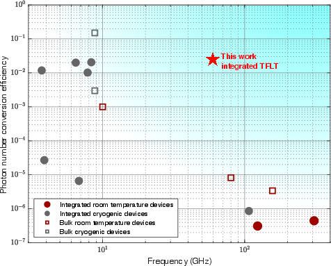
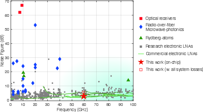
- Rydberg atom-based receivers: Microwave/THz receivers using highly excited atomic states with extreme field sensitivity. "Green triangles indicate Rydberg atom-based receivers~"
- rotatingâwave approximation: An approximation that neglects rapidly oscillating terms in the interaction Hamiltonian. "under the rotatingâwave approximation"
- scattering matrix: A matrix mapping input fields to output fields, characterizing reflection and transmission between ports. "Then we can define the scattering matrix as:"
- shot noise: Fundamental quantum noise arising from the discreteness of charge or photons. "it accumulates twice the shot noise"
- single photon electro-optic coupling rate: The interaction rate g0 between modes due to the EO effect at the single-photon level. "where $g_{\mathrm{0}$ is the single photon electro-optic coupling rate"
- transmission line resonator: A resonant structure formed by a length of transmission line with boundary terminations (e.g., shorts). "The optimal transmission line resonator employing a CPW geometry is terminated by short-circuits on either end"
- vacuum coupling rate: The single-photon coupling strength (g0) between fields in the absence of drive, set by field overlaps. "The vacuum coupling rate is obtained via calculation of the 3D overlap integral"
- whispering-gallery mode (WGM) resonators: Optical resonators where light circulates along the periphery due to total internal reflection, supporting high-Q modes. "bulk devices based on whispering-gallery mode (WGM) resonators"
Collections
Sign up for free to add this paper to one or more collections.