- The paper demonstrates voltage-tunable superconductivity via gate-controlled Josephson junctions on Ge quantum wells with an in-situ Al interface.
- It employs a deep mesa etch process and MBE-grown Ge QWs, achieving a peak critical current of 103 nA and an ICRN product of 8.63 μV.
- Interface analysis confirms ballistic transport and moderate transparency (4%-9%), paving the way for scalable hybrid superconducting circuits.
Introduction
Voltage-tunable Josephson junctions (VT-JJs) have emerged as essential elements for enabling electrical tunability in superconducting quantum circuits. Their electrostatic control over the Josephson energy addresses significant engineering limitations—specifically, the elimination of flux-controlled tuning and the associated flux noise, as well as integration challenges with scalable, low-loss superconducting platforms. This work presents the fabrication, characterization, and analysis of VT-JJs formed on planar germanium quantum wells (Ge QWs) with in-situ aluminum (Al) contacts, focusing on advances towards monolithic integration for quantum computation and superconducting electronic devices.
The junctions are realized on Ge QWs grown by molecular beam epitaxy (MBE) on float-zone silicon substrates, which are characterized by low microwave loss tangents (≤10−6). A layer sequence comprising a SiGe reverse-graded buffer, a 16 nm Ge quantum well, and SiGe spacers is terminated with a 1 nm Si cap. Without breaking vacuum, a 50 nm Al film is deposited in-situ to ensure an oxide-free interface, essential for coherent proximity effects and minimized interface disorder.
A key technological development in this work is a deep mesa etch process: after device definition, epitaxial material is removed except beneath the VT-JJ. This process achieves a tapered sidewall (18° from normal) that supports continuous deposition of metal interconnects and gates from the substrate up to the junction, facilitating the hybrid integration of low-loss microwave elements directly on the Si substrate.
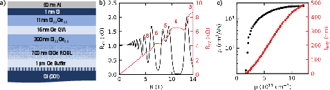
Figure 1: (a) Schematic of the Al/Ge QW heterostructure; (b) Magnetotransport in Hall bar geometry at 2 K, showing integer quantum Hall behavior; (c) Mobility and mean free path vs carrier density, with peak values of $26,800$ cm2/Vs and $482$ nm, respectively.
Materials Characterization
Transport in the Ge QWs exhibits high mobility and ballistic behavior, as validated through gated Hall bar measurements and observation of integer quantum Hall plateaus at B=11 T. The Ge QW peak mobility is $26,800$ cm2/Vs at a hole density of 1.2×1012 cm−2, and the associated mean free path (lmfp) reaches $26,800$0 nm. These metrics, comparable to state-of-the-art CVD-grown QWs, indicate that MBE-grown interfaces are predominantly limited by interface quality rather than bulk disorder or parallel conduction. The mean free path substantiates the viability of fabricating JJs that sustain ballistic supercurrents.
Structural and Interface Analysis
Scanning electron microscopy (SEM) and atomic-resolution high angle annular dark field (HAADF) scanning transmission electron microscopy (STEM) are used to analyze device structure and interfaces. The mesa profile shows continuous gate coverage, and STEM images reveal abrupt Ge/SiGe and Al/Si interfaces, with typical thicknesses of $26,800$1–$26,800$2 nm (Ge interfaces). Energy dispersive X-ray spectroscopy (EDS) confirms the absence of significant chemical intermixing at the metal-semiconductor interfaces, indicative of successful process control and minimal junction disorder.
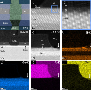
Figure 2: (a) SEM of the fabricated JJ with continuous gate ascent up the mesa; (b-d) HAADF STEM images highlighting clean interface morphology; (e-i) EDS maps highlighting elemental distribution, showing negligible intermixing.
Electrical Characterization
Low-temperature ($26,800$3 mK) DC transport measurements demonstrate robust gate-tunability of the supercurrent. The $26,800$4–$26,800$5 characteristics display a transition from a resistive state to a gate-activated supercurrent branch, with the critical current ($26,800$6) peaking at $26,800$7 nA for $26,800$8 V. Beyond this optimal gate voltage, $26,800$9 decreases, attributed to reduced QW mobility from the quantum-confined Stark effect or enhanced intersubband scattering at large electric fields.
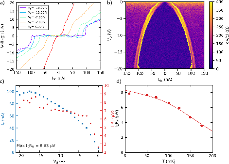
Figure 3: (a) 20–21 curves at 10 mK, demonstrating gate-tunable superconductivity; (b) Differential resistance map (22) vs bias current and gate voltage, with the maximum 23 at 24 V; (c) Gate dependence of 25 and 26 product; (d) Temperature dependence of 27 and fit to the Kulik-Omelyanchuk model.
The 28 product, a key figure of merit for interface transparency, achieves a maximum value of 29V at peak $482$0. This value, while comparable to ex-situ Al-Ge devices with deep Ge QWs, is considerably below the ideal theoretical value ($482$1), indicating moderate interface transparency. Fitting the temperature dependence of $482$2 with the generalized Kulik-Omelyanchuk model extracts interface transparencies of approximately $482$3–$482$4. The limiting factors for transparency are attributed to the presence of a relatively thick SiGe spacer and the absence of post-growth annealing, which could potentially further interdiffuse the superconductor-semiconductor interface but at the risk of compromising gap uniformity.
Integration and Practical Considerations
The deep mesa etch architecture enables the co-integration of VT-JJs with other superconducting elements on the same low-loss Si substrate, thus addressing a persistent limitation of hybrid superconductor-semiconductor qubit platforms—namely, microwave loss due to the buffer or heterostructure layers. The measured critical currents and tunable $482$5 support operation in the transmon regime ($482$6–$482$7), allowing frequency tuning between $482$8 GHz and $482$9 GHz. This is suitable for dispersive circuit QED implementations and scalable architectures.
The preservation of interface abruptness without annealing mitigates issues observed in earlier works, such as junction length non-uniformity due to metal diffusion, while the in-situ Al deposition minimizes oxide formation and associated B=110 noise sources. However, further improvement in interface transparency and coherence will require optimization of the barrier thickness and possibly alternative contact strategies (e.g., silicide/germanosilicide formation [tosato_hard_2023] for near-unity transparency).
Theoretical and Future Directions
The demonstrated scalable integration and voltage tunability of these JJs are poised to facilitate the development of hybrid quantum circuits, including gatemon and Andreev qubits with enhanced electrostatic control. The architecture is compatible with recent advances in planar QW spin qubits and protected superconducting circuits, enabling hybrid designs that could combine spin, charge, and phase degrees of freedom on a shared platform. Additionally, further reduction of loss and improvement of coherence times depend on continued progress in materials purification, interface engineering, and device design, with the potential for integrating protected cosB=111 or diode-based quantum devices [valentini_parity-conserving_2024].
Conclusion
This work establishes a reproducible protocol for fabricating voltage-tunable Josephson junctions on MBE-grown Ge QWs with in-situ Al contacts and scalable, low-loss integration via deep mesa etches. The JJs exhibit ballistic transport, gate-tunable supercurrent up to B=112 nA, and an B=113 product of B=114V with interface transparencies in the range of B=115–B=116. Although these devices do not reach the ideal transparency limit, the process flow provides a robust platform for scalable integration of hybrid superconducting circuits and suggests clear avenues for further improvement. This platform is expected to significantly impact the practical realization of voltage-tunable, monolithically integrated superconducting quantum architectures.

