- The paper establishes a deterministic, high-yield method for creating GeV centers using focused ion beam implantation and ultrahigh-temperature annealing.
- It reports formation yields up to 33% at optimal fluences, marking an order of magnitude improvement over previous methods.
- The study confirms single-photon emission from shallow GeV centers, paving the way for scalable integration into quantum photonic devices.
High-Yield Engineering of Germanium Vacancy Centers in Diamond via Focused Ion Beam Implantation and High-Temperature Annealing
Introduction and Motivation
Defect centers in diamond, particularly group IV (G4V) vacancy complexes, play a pivotal role in quantum information processing, quantum communications, and advanced photonic applications due to their robust spin and optical properties. The negatively charged germanium-vacancy (GeV) center has emerged as a strong candidate for these applications, owing to its inversion symmetry, high spectral stability, strong zero-phonon line (ZPL) emission at 602 nm, and exceptional electron and nuclear spin coherence times. However, scalable quantum device integration necessitates deterministic placement of GeV centers with high yield and spatial precision—requirements unmet by stochastic or uncontrolled creation techniques.
This work establishes a systematic and highly efficient process for the localized fabrication of GeV centers in diamond using focused ion beam (FIB) implantation of germanium ions, followed by ultrahigh-temperature annealing (up to 1500 °C). The study not only reports formation yields dramatically surpassing previous methods (up to 33%), but also achieves the controlled creation of shallow GeV centers at sub-10 nm depths, enabling compatibility with nanophotonic architectures.
Experimental Methodology
A polished type IIa (100)-oriented diamond substrate served as the host platform. Germanium ions were selectively implanted using a Raith Velion FIB system equipped with a AuGeSi liquid metal alloy ion source. Four distinct implantation energies (5, 10, 35, 70 keV) were utilized, with local fluences spanning 10–2000 ions per spot. Estimated mean penetration depths ranged from 5.5 nm (5 keV) to 29.8 nm (70 keV), with corresponding lateral straggling of 2–7 nm, optimized for spatial resolution and quantum device alignment.
The as-implanted substrate underwent rigorous triacid cleaning and was annealed in a high-vacuum environment employing a two-stage temperature sequence: 2 hours at 1200 °C, followed by 1 hour at 1500 °C. This sequence is specifically designed to maximize vacancy mobility and lattice healing, facilitating efficient formation of optically active GeV centers while mitigating graphitization and other amorphization effects.
A custom-built confocal photoluminescence (PL) setup, incorporating off-resonant 532 nm excitation and single-photon detection, was employed for exhaustive site-by-site characterization.
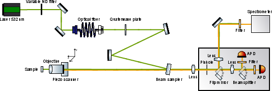
Figure 1: Schematic of the confocal setup for excitation and collection of GeV center emission, using fiber-coupled 532 nm CW laser and avalanche photodiodes for PL and correlation measurements.
Optical Verification and Single-Photon Assessment
PL mapping across all implanted regions unequivocally confirmed the generation of GeV centers at all energies. The characteristic ZPL at 602 nm was observed in every region, including for shallow implants at 5.5 nm depth.
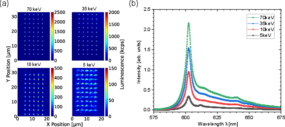
Figure 2: Left: PL maps from arrays implanted at various energies, with pronounced spot definition at higher energies. Right: All spectra exhibit the GeV zero-phonon line at 602 nm, confirming successful defect creation.
Assessment of individual spots in the low-fluence regime (10–50 ions/spot) at 35 and 70 keV energies routinely yielded isolated single GeV centers. Second-order autocorrelation g(2)(0) measurements for these sites registered clear antibunching dips below 0.5, providing stringent evidence for single-photon emission suitable for quantum applications. The best-performing single centers demonstrated saturated count rates of approximately 25 kcps and saturation excitation powers Psat∼1.15 mW.
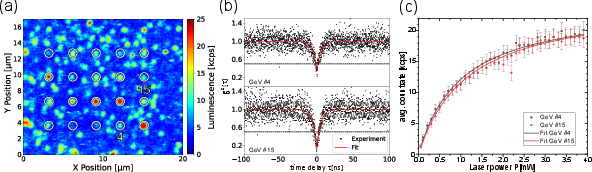
Figure 3: (a) PL map for sites implanted at 70 keV and 10 ions/spot. (b) g(2)(τ) autocorrelation for two single GeV centers with g(2)(0)<0.5. (c) Saturation curves for these centers—indicative of stable, bright emission.
Two independent methodologies were applied to determine the GeV formation yield: (1) the photon yield method, benchmarking spot intensity against single-center reference emission, and (2) the integrated 2D PL map analysis, enabling robust extraction of total GeV content even when emission is spatially extended.
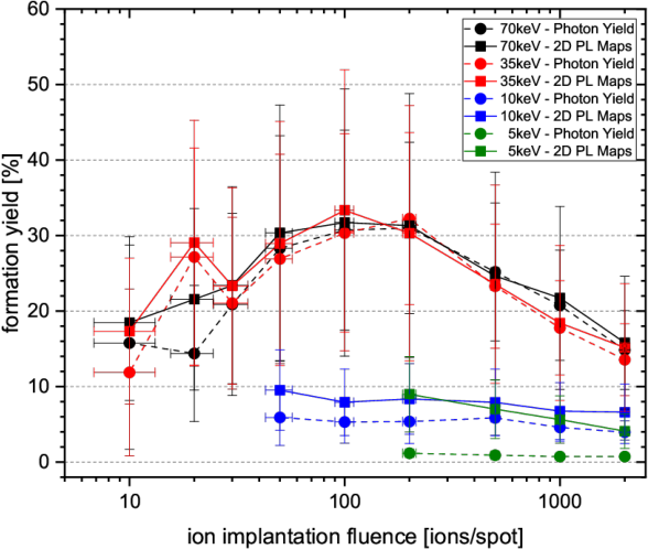
Figure 4: Formation yield as a function of fluence at all energies, comparing photon yield (dots) and 2D PL map (squares) methodologies.
Key findings include:
- High-Energy Regimes (35, 70 keV): Formation yields exhibited strong fluence dependence: at low fluence (10 ions/spot), yields were 15–17%, peaking at 31–33% for 100–200 ions/spot, then declining at very high fluence (≥2000 ions/spot) due to lattice amorphization and graphitization side effects.
- Low-Energy Regimes (5, 10 keV): Lower yields were observed (6–8%), relatively fluence-independent. These yields are still significantly enhanced compared to prior reports for similar depth regimes, attributed to optimized annealing and clean FIB conditions.
Both methods converged for well-confined, high-energy sites, but the 2D PL map method better captured yields for partially delocalized/larger spots at low energies.
Discussion
The observed maximum formation yields in this work—exceeding 30% for focused, well-aligned FIB sites at high energy—are at least an order of magnitude greater than previously reported values for GeV formation in diamond (2606.28528). This is attributed to the synergistic effect of (a) highly localized ion implantation with minimal lateral straggling, and (b) annealing at 1500 °C, which greatly enhances vacancy mobility and defect activation. At the same time, the process preserves sub-diffraction-limited placement, critical for scalability in integrated photonics.
The fluence-dependent nonlinearity in yield, with maxima at moderate fluence, corroborates theories that vacancy density and nanoscopic lattice damage mediate defect complex creation but that excessive local damage can suppress yield by amorphization or graphitization. The results imply a clear optimization window for balancing defect creation and lattice preservation.
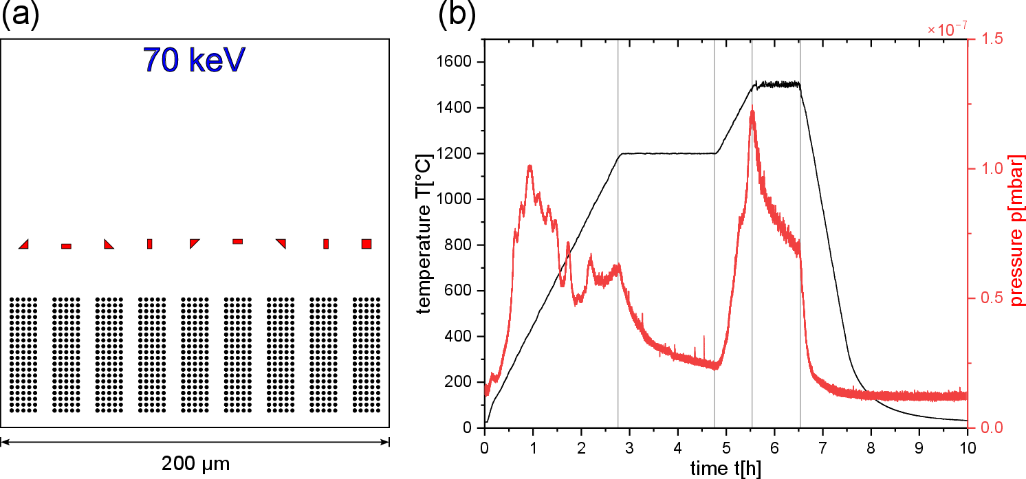
Figure 5: (a) Implantation map for 70 keV region, color-coded by fluence and marker locations. (b) Pressure and temperature trace for the two-step annealing cycle.
The reliable generation of shallow (5.5 nm) GeV centers at >6% yield represents a distinct advance for surface-proximal quantum sensing modalities and for integration of GeV sites into high-field photonic nanostructures and waveguides.
Implications and Future Developments
This method sets a new benchmark for engineered color centers in diamond, combining high spatial selectivity, unrivaled formation efficiency, and compatibility with nanophotonic device integration. The deterministic fabrication at defined depths and lateral positions opens the path for scalable quantum network node arrays, on-chip single-photon sources, and spin-based quantum registers.
Anticipated directions for future research include:
- Integration of GeV arrays into photonic crystal cavities, pillars, or waveguides for cavity QED and multiplexed quantum-light sources.
- Extension to hybrid defect-ensemble devices where high-yield, shallow placement is crucial for magnetic, electric, or strain sensing and information transduction.
- Exploration of further annealing optimization, co-implantation strategies, or strain engineering to increase yield and tailor spectral properties.
Conclusion
This study demonstrates an optimized protocol for the creation of GeV centers in diamond with record-high formation yields up to 33% using focused ion beam implantation coupled to high-temperature annealing. The process enables <30 nm spatial placement precision, shallow depth control, and compatibility with industrial-scale nanofabrication, and surpasses previous methods both in efficiency and technological applicability. The results directly support scalable quantum photonics and sensing applications built on G4V color centers.

