- The paper demonstrates that the μ-MOPA laser decouples low-threshold oscillation from power scaling by combining a microring master oscillator with a Nd:YAG spiral amplifier for enhanced conversion efficiency.
- It achieves record small-signal gain exceeding 46 dB and pump-to-signal conversion efficiency up to 52%, while maintaining low absolute noise and high spectral purity.
- Experimental results show robust performance against pump detuning and scalability to >15 mW output in two-stage systems, enabling integration in diverse photonic applications.
μ-MOPA Architecture for Photonic Integrated Solid State Laser: Technical Analysis
Introduction
This work presents a photonic-integrated master-oscillator–power-amplifier (μ-MOPA) laser system based on directly bonded single-crystal Nd:YAG on silicon nitride (Si₃N₄) waveguides. The architecture leverages the high gain efficiency and stability of diode-pumped solid-state (DPSS) Nd:YAG lasers, now implemented on a scalable, low-loss chip platform. By architecting the laser as a cascaded system with a separate, low-threshold master oscillator and one or more high-gain waveguide amplifiers, the μ-MOPA configuration enables both low absolute noise and high output power, overcoming fundamental limitations of single-resonator on-chip lasers.
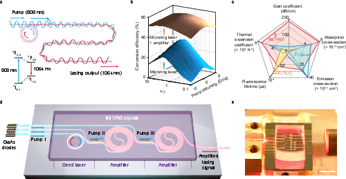
Figure 1: Chip-integrated Nd:YAG μ-MOPA lasers, including device schematic, pump-to-signal conversion efficiency surfaces under varying coupling and detuning, gain-material benchmarking versus Ti:Sa and Er:Si₃N₄, and micrograph of fabricated device.
Motivation and Context
While DPSS lasers such as Nd:YAG are well established for applications necessitating efficient, narrow-linewidth sources—spanning metrology, quantum optics, medical diagnostics, and more—their bulk, free-space architectures preclude integration into photonic circuits. By contrast, semiconductor-based integrated lasers and amplifiers remain limited in gain, efficiency, spectral coverage, or coherence. Recent on-chip rare-earth integration efforts have targeted Ti:sapphire and Er-doped platforms, but both suffer from either limited gain efficiency or spectral constraints.
This work addresses the persistent challenge of combining the quantum-defect-limited conversion efficiency and four-level system operation of Nd:YAG with monolithic photonic platforms, ultimately delivering chip-scale DPSS sources capable of high power and robust spectral performance.
μ-MOPA System Architecture and Modeling
The μ-MOPA laser employs a two-element cascade: a double-resonant Si₃N₄ microring master oscillator (seed) and a single-pass Nd:YAG amplifier stage (or stages), each independently pumped at 808 nm. The microring resonator is designed for simultaneous critical coupling at both pump and signal wavelengths, maximizing internal conversion while facilitating mode purity and cavity finesse. The amplifier, implemented as a spiral waveguide, achieves efficient pump-to-signal overlap and gain length within the tight photonic circuit footprint.
The conversion efficiency landscape, modeled as a function of pump detuning and resonator coupling conditions, clearly shows that while single-ring operation yields a narrow optimal regime, the μ-MOPA configuration achieves substantially higher and more robust conversion efficiency across a realistic parameter space for chip fabrication and packaging tolerances.
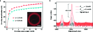
Figure 2: Amplification characteristics of integrated Nd:YAG waveguide amplifiers, demonstrating up to 46.6 dB net gain from a 2.3-cm spiral with 12 mW pump, and ASE suppression >40 dB.
Standalone Nd:YAG amplifiers, realized as tightly confined spiral waveguides, serve as the power-scaling backbone of the μ-MOPA system. The measured small-signal gain exceeds 46 dB for a 2.3-cm-long, 2 μm-wide spiral, which is a record among integrated single-chip rare-earth and transition-metal doped amplifiers. The signal-to-ASE contrast exceeds 40 dB, and the lack of parasitic lasing across the gain medium is confirmed. Pump-to-signal conversion efficiency in the large-signal regime reaches 52%, with intrinsic amplifier efficiency (excluding insertion/coupling losses) approaching 72%—within 10% of the quantum defect limit set by the Nd:YAG energy diagram.
Experimentally extracted losses for both pump and signal are mainly the result of mode mismatch at interfaces, and deployment of next-generation spot-size converters is projected to further improve these values.
Master Oscillator Design: Microring Seed Laser
The master oscillator utilizes a dual-resonant (808 nm and 1064 nm) microring, with independent optimization for threshold and output coupling. Under high-Q, under-coupled conditions, thresholds as low as 2.9 μW are achieved. In the alternate, over-coupled configuration, slope efficiency from a single port reaches 34%. Double resonance ensures near-unity pump and signal mode overlap, tight spatial confinement, and robust performance against pump detuning. Intracavity loss measurements confirm Q-factors exceeding 2.5 million at 1064 nm.
Longitudinal mode purity is verified by heterodyne and self-heterodyne measurements, yielding intrinsic linewidths around 16 kHz even after cascaded amplification, indicating that the amplifier does not degrade spectral coherence.
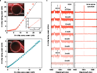
Figure 3: Microring master oscillator performance, showing threshold and slope efficiency under distinct coupling regimes, and preservation of single-mode operation confirmed via OSA and heterodyne analysis.
μ-MOPA System Integration and Results
Cascading the master oscillator with one or more amplifier stages, the integrated μ-MOPA achieves >12 dBm (15 mW) continuous-wave output in a two-stage configuration, a threefold improvement over the single-ring design. The modular architecture enables power scaling by incrementally adding amplifiers, with modeling indicating >40 mW output is feasible with eight amplifier stages.
Conversion efficiency (P_signal/P_pump) saturates near the theoretical maximum with careful optimization of pump power distribution between oscillator and amplifiers, exceeding 68% in the best configurations. Notably, the μ-MOPA system demonstrates stable efficiency and output across variations in pump detuning and coupling, circumventing the sensitivity of single-cavity designs.
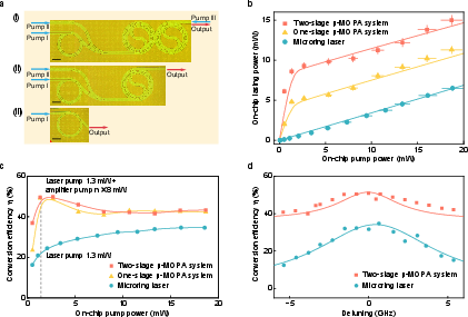
Figure 4: System-level μ-MOPA results: device topologies, power scaling with amplifier stages, conversion efficiency versus pump power, and resilience to pump-cavity detuning.
Practical and Theoretical Implications
The μ-MOPA system realizes, for the first time on chip, the decoupling of low-noise, low-threshold lasing and power scaling, removing the trade-off—imposed by critical coupling analysis—between pump utilization and signal extraction in single-resonator geometries. The bonded Nd:YAG layer, integrated via room-temperature processes, demonstrates robust long-term operation without degradation in gain, threshold, or slope efficiency.
Practically, this architecture enables monolithic, high-coherence, and power-scalable DPSS sources suitable for quantum photonics, precision metrology, on-chip clocks, and high-demand spectroscopic systems. The μ-MOPA approach is readily generalizable to other high-gain crystalline or amorphous platforms (e.g., Ti:sapphire, Er:Yb:LN, Al₂O₃:Nd), expanding the accessible spectral and power regimes for integrated photonic applications. Heterogeneous integration of improved edge couplers, thermal management for high-brightness operation, and advanced pump recycling strategies will push electrical-to-optical wall-plug efficiency closer to theoretical limits.
On the theory side, the modular system elucidates the intrinsic gain dynamics and pump-signal interaction in tightly confined, high-Q environments, providing a new testbed for four-level rare-earth kinetics at the chip scale.
Future Outlook
Power scaling via additional amplifier stages, the use of hybrid or monolithically integrated pump diodes, and deployment of custom spot-size or vertical couplers will further improve the absolute system output and efficiency. Additionally, advances in fast modulation or leveraging Si₃N₄ Kerr nonlinearities will expand applications to mode-locked or pulsed operation.
Broadly, the μ-MOPA architecture signals a critical advance in the integration of high-efficiency, low-noise solid-state gain materials with low-loss photonic platforms, bridging the gap between bulk DPSS performance and the demands of next-generation quantum and classical photonic systems.
Conclusion
This work establishes chip-scale Nd:YAG μ-MOPA lasers as a high-efficiency, power-scalable light source platform, demonstrating that heterogeneous bonding of bulk crystalline gain media to low-loss waveguides yields both quantum-defect-limited conversion and unmatched noise performance. By separating the roles of master oscillator and amplifier, the architecture realizes new operational regimes in integrated photonics, robust to device-level imperfections and fully compatible with modular scaling. These results provide a foundation for future development in on-chip solid-state sources tailored to precision applications at the convergence of classical and quantum technologies.

