Octave bandwidth 3D-Printed Couplers for Low-Loss Thin-Film Lithium Tantalate Circuits
Abstract: Low-loss, broadband photonic integrated circuits (PICs) are critical enablers for optical communications, photonic computing, and quantum applications. Lithium tantalate on insulator (LTOI) is an emerging photonic platform offering a wide transparency window and strong Pockels effect, and thereby enabling efficient electro-optic modulation and high data rates. Here, we present the first implementation of efficient out-of-plane polymer coupling interfaces fabricated via 3D direct laser writing for both fully etched strip and partially etched rib LTOI waveguides, achieving ultra-low coupling losses of 0.9 dB (strip) and 1.25 dB (rib) per interface. Both coupler types exhibit a 3 dB optical bandwidth spanning more than an octave from 850 nm to 1740 nm and maintain stable operation under 1 W optical input power. Combined with on-chip waveguides exhibiting propagation losses below 0.1 dB/cm, these characteristics represent a key step toward unlocking the full potential of LTOI for high-speed optical signal processing with an unprecedented degree of parallelism. In addition, the octave-spanning bandwidth enables efficient interfacing of both the fundamental and second-harmonic signals, making the platform highly attractive for second harmonic generation based quantum squeezing applications.
Paper Prompts
Sign up for free to create and run prompts on this paper using GPT-5.
Top Community Prompts
Explain it Like I'm 14
What this paper is about (in simple terms)
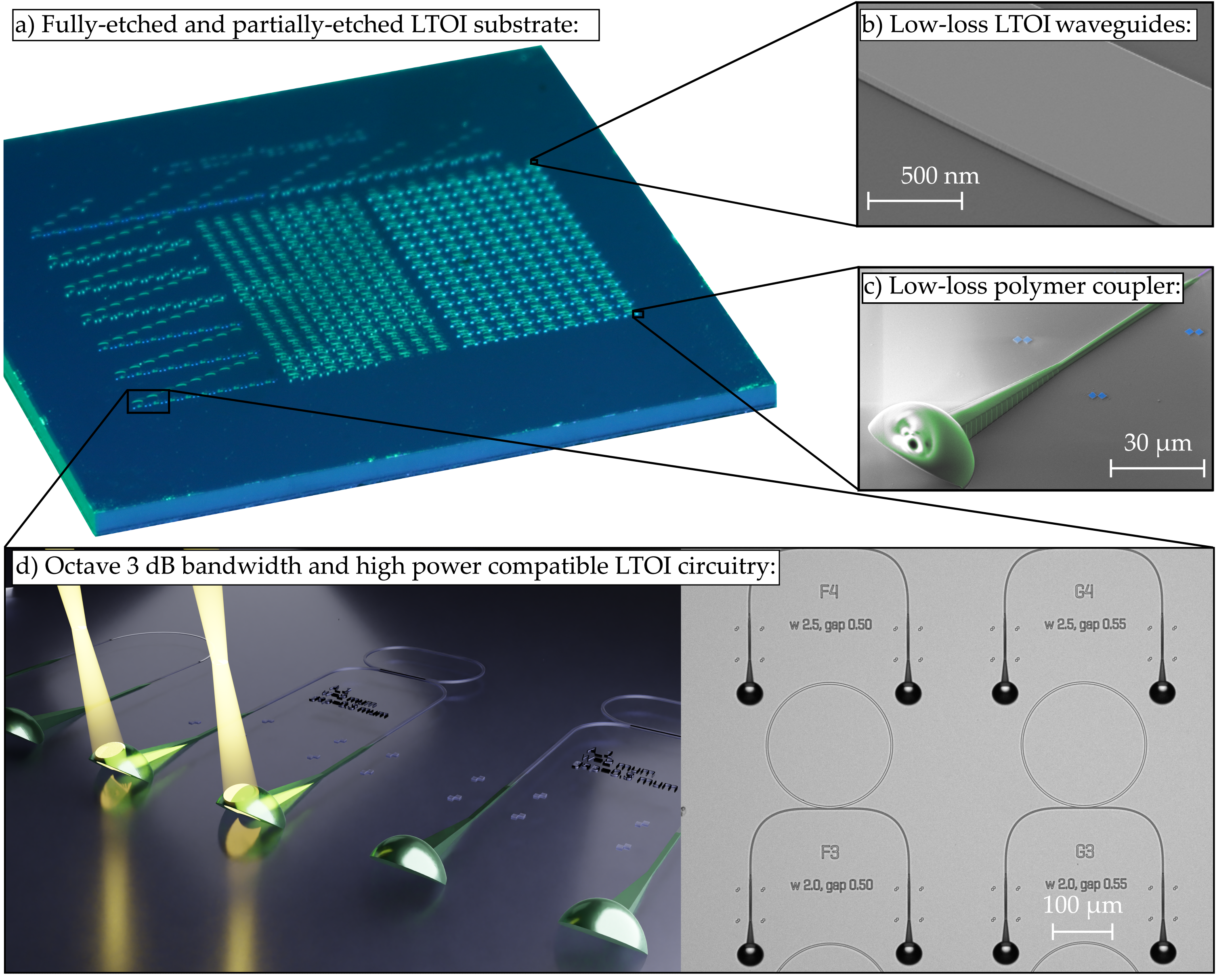
This paper shows a new, very efficient way to connect optical fibers to tiny light circuits on a chip made from lithium tantalate (a crystal). Think of the chip as a city of “light roads” (waveguides) that carry information. To get light into and out of that city, you need good “on-ramps” and “off-ramps.” The authors 3D‑print microscopic ramps and mirrors (called couplers) directly on the chip so light can flow smoothly between a fiber and the chip with very little loss, across a very wide range of colors.
The main goals and questions
The researchers wanted to:
- Build tiny, 3D‑printed “bridges” that connect standard optical fibers to two common types of light-guiding paths on the chip (called strip and rib waveguides).
- Make these bridges work over an extremely wide color range (from near‑visible red to infrared) so one design can handle many colors at once.
- Keep losses very low, so not much light is wasted.
- Prove the system can handle high power without breaking.
- Show that the on‑chip “roads” themselves are also very low loss.
How they did it (explained with everyday ideas)
- Photonic chips and waveguides: Imagine narrow glassy roads on a chip that guide light like lanes guide cars. There are two road shapes:
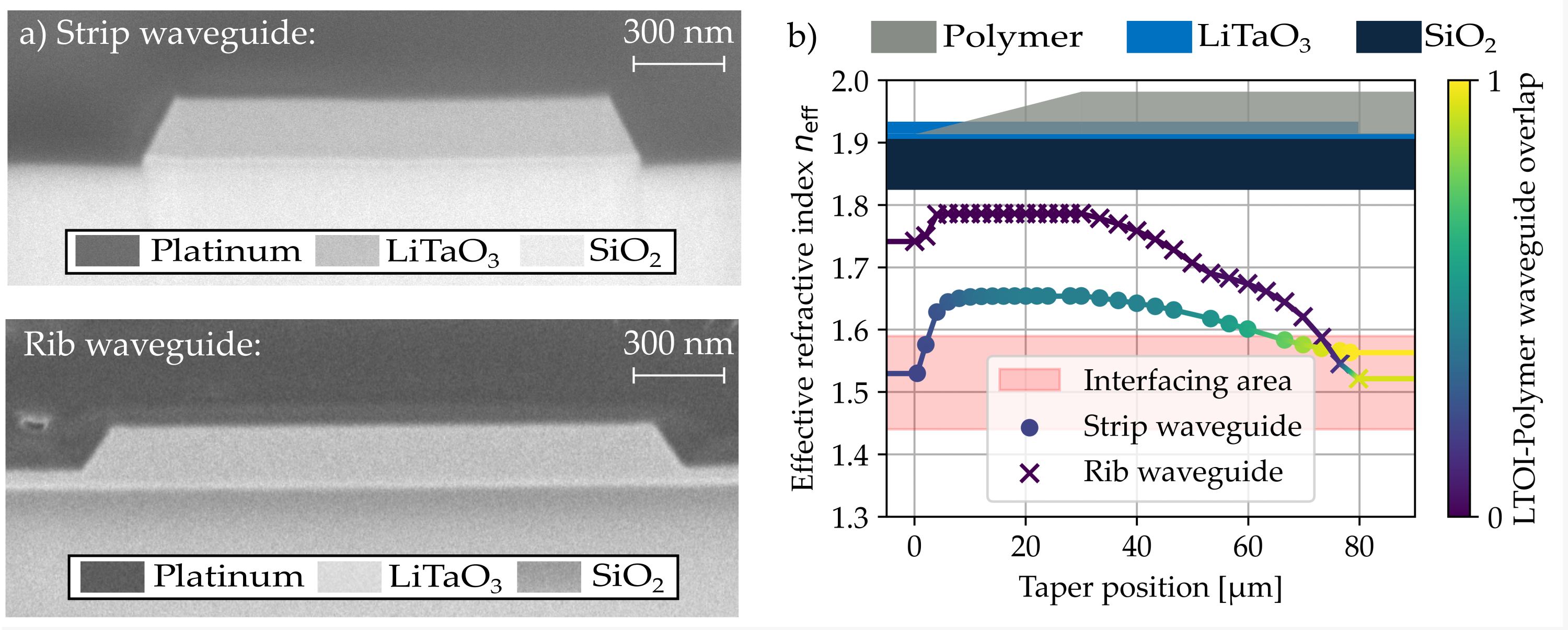
- Strip waveguides: deeply carved, like trenches.
- Rib waveguides: partially carved, like a raised lane with a shallow trench beside it. These are useful for fast “traffic lights” that modulate light (electro‑optic modulators).
- 3D‑printed couplers: Using a very precise laser “3D printer,” the team printed tiny polymer structures right on top of the chip’s roads. Each coupler is like a miniature periscope made of:
- A gentle “ramp” (a taper) that gradually shifts the light from the chip road into a small polymer road on top—like merging lanes so cars don’t crash.
- A “mirror” that uses total internal reflection (TIR) to bend the light upward out of the chip—like bouncing a beam off a shiny wall.
- A tiny lens that focuses the beam so it matches a standard optical fiber.
- Matching materials so light stays on track: The chip’s crystal (lithium tantalate) bends light more than the printed polymer does. To move light smoothly from the chip road into the polymer road, they narrow the chip road so the light “prefers” the polymer. For rib waveguides (with a leftover slab underneath), they switched to a slightly higher‑index polymer so the light wouldn’t leak into the slab—like choosing the right pavement so cars don’t slip into a side lane.
- Measuring performance:
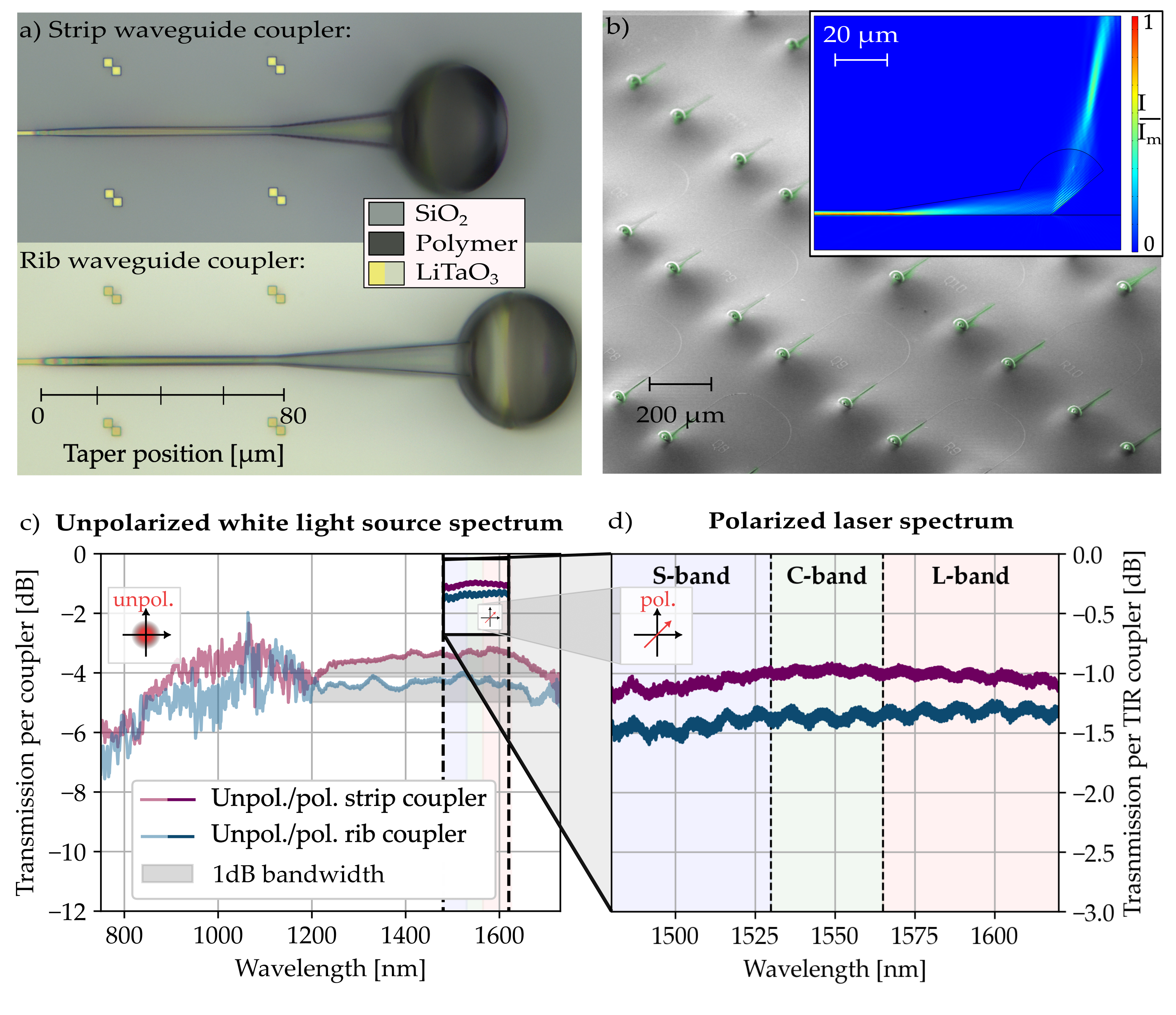
- They shined a white light (many colors) and a tunable laser (selectable color) through the couplers to see how much light gets through at different colors.
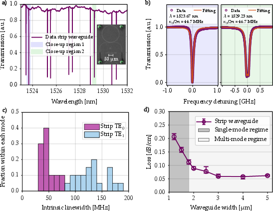
- They built ring resonators (loops of waveguide) to measure how much loss happens along the on‑chip roads themselves.
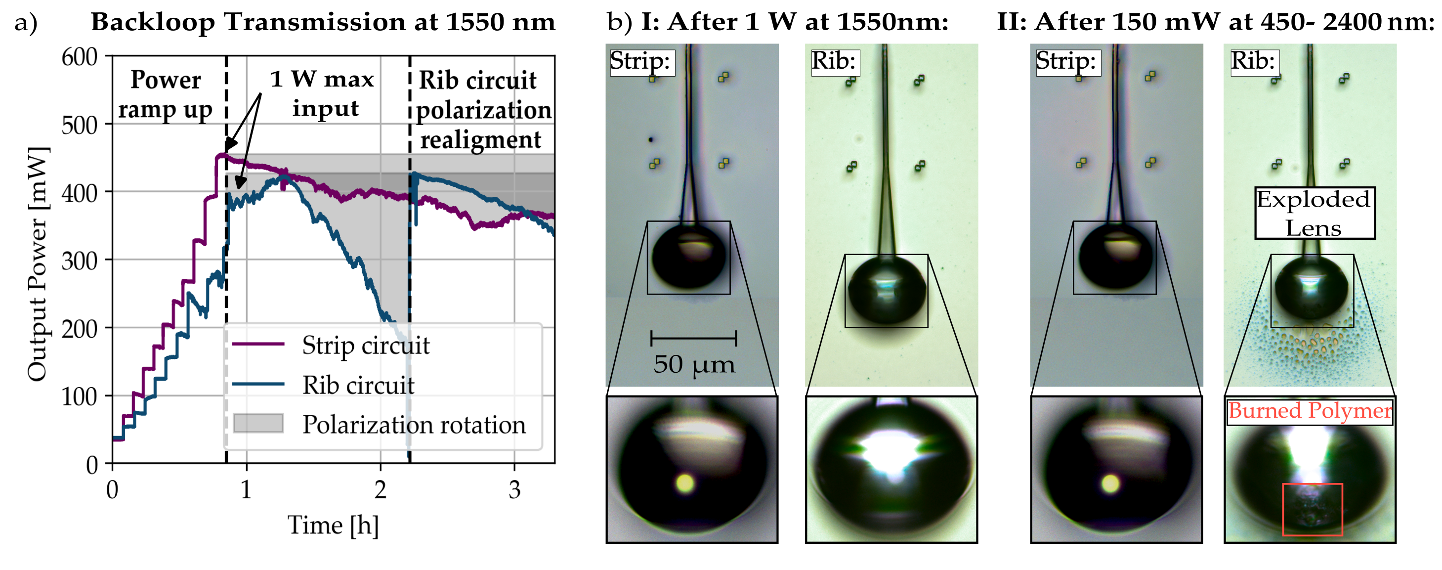
- They tested power handling by sending strong laser light (up to 1 watt) to see if anything breaks.
What they found and why it matters
Here are the key results:
- Very low coupling loss:
- About 0.9 dB loss per coupler for strip waveguides.
- About 1.25 dB loss per coupler for rib waveguides.
- (Lower dB means less light lost. These are strong results—less than ~20–25% loss at each connection.)
- Huge color range (bandwidth):
- The couplers work well from about 850 nm to 1740 nm. That’s more than an “octave,” like going from one musical note to the same note an octave higher—twice the frequency. In color terms, it’s a very wide slice of the rainbow.
- Over this range, the power only drops by a small, controlled amount (1–3 dB across hundreds of nanometers), which is much broader than many common couplers.
- Low loss on the chip:
- The waveguides themselves have very low loss: about 0.06–0.11 dB per centimeter. That means light can travel longer distances on the chip without fading much.
- High power handling:
- The couplers and waveguides survived 1 watt of infrared light at 1550 nm for 2 hours with no visible damage—great for systems that need strong light.
- One of the polymers used for rib waveguides doesn’t like high power at visible wavelengths (it can heat and get damaged), but it’s fine in the infrared where it’s meant to operate.
Why this is important:
- Faster, broader, and simpler connections: One coupler design that works for many colors means simpler, cheaper, and more flexible optical systems.
- Works with key waveguide types: Success with rib waveguides is big because rib designs are used for fast electro‑optic modulators (the “traffic lights” that switch and encode light quickly).
- Helpful for quantum optics: The broad range covers both a fundamental color and its second harmonic (double the frequency), making it easier to build devices for quantum squeezing and other advanced light tricks.
What this could lead to
- High‑speed communications: These couplers can help build low‑loss, multi‑color optical networks on a chip, moving lots of data quickly and efficiently.
- Photonic computing: Better, low‑loss connections and roads (waveguides) are essential for optical processors that do math with light.
- Quantum photonics: The ability to handle both a color and its doubled color helps create and measure special quantum states of light, supporting more stable and scalable quantum experiments.
- Easier testing and manufacturing: Because the couplers point out of the chip, many devices on a wafer can be tested quickly without polishing chip edges, speeding up development.
In short, the team built tiny 3D‑printed “periscopes” that connect fibers to lithium tantalate chips with very low loss and across a huge color range—even at high power. This is a strong step toward faster, more capable optical and quantum technologies.
Knowledge Gaps
Knowledge gaps, limitations, and open questions
Below is a concise list of missing, uncertain, or unexplored aspects that, if addressed, could strengthen or extend the work.
- Polarization dependence: The couplers show ≈3 dB variation between unpolarized and TE-polarized measurements; polarization-resolved loss (TE vs TM), extinction ratio, and a strategy for polarization-insensitive or polarization-diverse coupling are not provided.
- Visible-wavelength power handling for rib couplers: IPN-162-based rib couplers fail under 150 mW broadband illumination; the absorption spectrum, damage thresholds, and thermal/photochemical damage mechanisms of IPN-162 (and alternatives) across 450–900 nm remain uncharacterized.
- Long-term reliability and environmental stability: Only a 2-hour, 1 W test at 1550 nm is shown; lifetime under continuous high power, thermal cycling, humidity/UV exposure, and mechanical vibration/shock is not assessed for either resin or the LTOI–polymer interface.
- Temperature dependence: The thermo-optic and thermal-expansion impacts on coupling efficiency, focal position, and return loss over a practical operating range (e.g., −40 to 85 °C) are not measured.
- Alignment tolerance and packaging: Lateral/vertical/angular 1 dB/3 dB alignment windows to the fiber and tolerance to fiber-array pitch errors are not quantified; no mechanical packaging scheme or robustness data for the 3D structures are provided.
- Back-reflection/return loss: The optical return loss from the TIR surface and lens is not reported; its impact on laser coherence, resonator ripples, and interferometric or quantum applications is unknown.
- Phase and dispersion response: Spectral phase, group delay, and chromatic aberrations of the couplers across the octave are not characterized; these are critical for coherent systems, ultrashort pulses, and squeezing experiments.
- SHG-relevant dual-wavelength performance: Absolute, polarization-controlled insertion loss at both the fundamental (e.g., 1550 nm) and second harmonic (e.g., 775 nm) is not reported; simultaneous bidirectional coupling of both wavelengths and corresponding mode/NA matching are not validated experimentally.
- TM-mode support: Only TE-mode operation is demonstrated; coupling efficiency, bandwidth, and polarization crosstalk for TM (and mixed polarization states) remain unknown.
- Wafer-scale manufacturability and yield: Throughput of 2PP printing (time per coupler, per wafer), placement/yield statistics, and between-die/within-die variability of coupling loss are not quantified.
- Coupler-to-coupler variability and process sensitivity: Loss spread vs printing voxel size, dose, development conditions, and waveguide dimensional variations (etch depth, sidewall angle, taper width) is not reported.
- Coupler spacing and crosstalk: Minimum pitch, scatter-induced crosstalk between adjacent couplers, and footprint constraints for high-port-count arrays are not analyzed.
- Material selection trade-offs: A systematic mapping of refractive index vs absorption vs bandwidth for candidate polymers (including dispersion data and loss spectra) is missing, especially for partially etched (rib) structures.
- Integration with active EO devices: The impact of electrodes/metal proximity, topography, RF fields, and potential heating on the printed couplers and mode-transfer tapers (and vice versa) is unexplored.
- Compatibility with upper claddings: Proposed upper-cladding approaches to lower waveguide loss may interfere with out-of-plane coupling; design rules and process flows for co-integration are not demonstrated.
- Performance at shorter wavelengths: While spectra extend to ~750–850 nm, there is no controlled, polarized loss measurement, nor analysis of slab-mode parasitics and sidewall scattering in the visible regime.
- Quantitative focusing/NA matching: Measured mode-field diameter and numerical aperture at the coupler output (and their wavelength dependence) are not reported; tolerance to fiber NA and MFD variations remains unknown.
- Mechanical/chemical robustness of printed optics: Scratch/abrasion resistance, solvent compatibility (post-packaging), outgassing, and vacuum/cryogenic behavior of the printed polymers are not characterized.
- High-peak-power operation: Only CW testing is provided; coupler and waveguide resilience to pulsed (high peak power) operation pertinent to nonlinear/quantum use cases is not evaluated.
- Extension beyond LTOI: Although applicability to thicker slabs or higher index-contrast platforms (e.g., LNOI) is suggested, no experimental validation or concrete design guidelines are given.
- Waveguide loss vs wavelength: Propagation loss is extracted around 1550 nm; loss dispersion, sidewall-scattering scaling, and mode-dependent loss across the demonstrated octave are not quantified.
- Backward/stray light management: Scattered light from the TIR facet and mode-transfer region (and its effect on on-chip detectors or neighboring circuits) is not assessed.
- Statistical reproducibility of ring resonator metrics: Loss/Q-factor sensitivity to coupler proximity and printed structure variability (coupler-induced loading or backscattering) is not separated from intrinsic waveguide performance.
- Metrology of 3D-printed surfaces: Surface roughness, facet flatness of the TIR mirror, and lens aberrations vs process parameters are not measured, preventing a loss budget breakdown.
- Design files and parameter sweeps: Open-source parametric designs, tolerance analyses, and optimization recipes for the mode-transfer taper and TIR geometry are not provided, hindering replication and adaptation.
- System-level demonstrations: End-to-end links with many parallel channels, simultaneous fundamental/SHG routing, or integration into a full EO-modulation/squeezing experiment are not shown, leaving application-level performance unverified.
Practical Applications
Immediate Applications
The following use cases can be deployed now using the paper’s demonstrated octave-bandwidth, low-loss (0.9–1.25 dB) out-of-plane 3D-printed couplers on low-loss LTOI waveguides (<0.1 dB/cm) with up to 1 W power handling at 1550 nm.
- Broadband wafer-level testing and characterization of LTOI PICs — industry, academia
- What: Rapid, probe-free I/O to devices across 850–1740 nm (including S/C/L telecom bands) for yield learning, process control, and broadband device metrology (rings, filters, modulators, SHG elements).
- Tools/products/workflows: Nanoscribe Quantum X align printing of TIR couplers aligned to on-chip markers; fiber-array probe cards with standard SMF; existing wafer probers; NPXPY job preparation.
- Assumptions/dependencies: Throughput of 2PP printing is sufficient for sample- or die-level testing; polarization management (TE preferred) is available; cleanroom access for coupler printing on processed wafers.
- Facetless fiber I/O for LTOI prototypes and lab systems — industry (R&D), academia
- What: Replace edge coupling and facet polishing with top-side, sub-dB couplers to accelerate prototyping of LTOI circuits (rings, MZIs, EOMs).
- Tools/products/workflows: Printable TIR coupler library cells for LTOI PDKs; standard SMF arrays; simple flip-chip or clamp fixtures.
- Assumptions/dependencies: Alignment markers on the die; availability of IPX-clear (strip) and IPN-162 (rib) resins; encapsulation strategy for environmental stability.
- Dual-wavelength interfacing for SHG-based squeezed-light experiments — quantum photonics (academia/industry)
- What: Couple both fundamental (e.g., 1550 nm) and second-harmonic signals (near 775–850 nm) through the same interface with small efficiency penalty, reducing asymmetry that limits squeezing levels.
- Tools/products/workflows: LTOI rings/waveguides with SHG sections; printed couplers characterized over 750–1730 nm; PM fibers and polarization control for TE excitation.
- Assumptions/dependencies: Operation near 775–850 nm at low-to-moderate power (rib-coupler resin shows reduced power tolerance in the visible); periodic poling or χ(2) engineering on LTOI as needed.
- High-power pump routing for nonlinear on-chip optics at 1550 nm — telecom, quantum, sensing (industry, academia)
- What: Reliable delivery and extraction of up to 1 W optical power at 1550 nm for parametric processes, frequency conversion, or pump-probe experiments without visible coupler damage over hours.
- Tools/products/workflows: EDFA-amplified sources; printed TIR couplers; LTOI low-loss waveguides; thermal monitoring.
- Assumptions/dependencies: Power tolerance validated at 1550 nm; visible/UV power must be limited for rib couplers using higher-index polymers.
- Broadband integrated spectroscopy and OCT-compatible PIC I/O — healthcare, industrial sensing (industry, academia)
- What: Use octave-spanning couplers for chip-based broadband sources/detectors in the 850–1300–1700 nm windows (e.g., OCT, NIR spectroscopy, chemical/biomedical sensing).
- Tools/products/workflows: LTOI spectrometer chips, interferometers; printed couplers; standard SMF interfacing.
- Assumptions/dependencies: Application power levels compatible with resin absorption at shorter wavelengths; use IPX-clear for better visible tolerance or alternative low-loss polymers.
- Drop-in upgrade for LTOI electro‑optic modulator testbeds — communications, photonic computing (industry, academia)
- What: Efficient fiber I/O to partially etched rib waveguides (needed for efficient Pockels modulation) using high-index polymer couplers (IPN‑162) for immediate modulator benchmarking.
- Tools/products/workflows: Printed couplers with mode-transfer tapers tuned for rib geometries; RF/electrode co-design unaffected by out-of-plane I/O.
- Assumptions/dependencies: Polarization control; process windows for rib etch and residual slabs; thermal management during high-speed operation.
- Rapid packaging for demos without facet polishing — industry (R&D), startups
- What: Demonstrators and pilots can be packaged with top-side couplers and fiber arrays, avoiding dicing/cleaving tolerances and facet quality constraints.
- Tools/products/workflows: Fiber-array attachment; UV-curable encapsulants; alignment jigs; epoxy/underfills compatible with printed polymers.
- Assumptions/dependencies: Mechanical protection of printed structures; environmental sealing for humidity/UV exposure; handling procedures.
- Educational and training kits for integrated photonics — education, workforce development
- What: Assemble teaching modules where students measure broadband PIC devices via robust, easy-to-align out-of-plane couplers.
- Tools/products/workflows: Pre-printed coupler-equipped chips; off-the-shelf tunable lasers/white-light sources; OSAs and photoreceivers.
- Assumptions/dependencies: Cost and availability of printed coupler chips; simplified polarization control included in kits.
Long-Term Applications
These opportunities require additional R&D in materials, scaling, or system integration (e.g., manufacturing throughput, robust packaging, or co-integration with active devices).
- High-volume LTOI transceivers and modulators with broadband fiber attach — communications, datacenters
- What: Product-grade transmit/receive modules leveraging low-loss LTOI Pockels modulators and octave-band couplers for wideband WDM and simplified packaging.
- Tools/products/workflows: Foundry PDK cells for couplers; high-throughput 2PP (multi-beam) or replication (nanoimprint) of polymer optics; automated fiber-array attach.
- Assumptions/dependencies: Long-term polymer stability (thermal, humidity, photo-oxidation), PM fiber support, Telcordia-grade reliability; supply chain for suitable low-absorption, high-index polymers.
- Multi-wavelength, massively parallel photonic compute/AI accelerators — computing, data centers, edge AI
- What: Exploit low-loss LTOI with fast EO modulation and octave-spanning I/O for dense WDM channels feeding on-chip matrix ops and neuromorphic blocks.
- Tools/products/workflows: Multi-λ microcombs, LTOI modulators, broadband I/O, control electronics; software stacks (e.g., PyTorch interfaces) adapted to photonic hardware.
- Assumptions/dependencies: Thermal stability, crosstalk control, polarization management at scale; standardized packaging; demonstrated system-level training/inference pipelines.
- Integrated quantum photonic networks and squeezed‑light sensors — quantum communications, metrology
- What: Chip-scale squeezed light generation and manipulation with simultaneous fundamental/SH coupling on a single port; low-loss circuits for entanglement distribution.
- Tools/products/workflows: Periodically poled LTOI, high-Q resonators, active EO control, broadband I/O; cryo/room-temperature-compatible packaging as needed.
- Assumptions/dependencies: Mature LTOI poling processes; balanced dual-wavelength coupling including <850 nm; low-loss at target wavelengths; noise management and stability.
- Heterogeneous photonic chiplet integration via 3D-printed photonic interposers — electronics/photonics co-packaging
- What: Bridge dissimilar platforms (InP lasers, SiN filters, LTOI modulators) using 3D-printed waveguides and out-of-plane TIR links for system-in-package optical routing.
- Tools/products/workflows: Photonic wire bonding extensions; automated 3D printing across multi-chip assemblies; co-designed optical/mechanical fixtures.
- Assumptions/dependencies: Precise 3D alignment at volume; low-loss bends and transitions; material sets with matched CTE and long-term reliability.
- Ruggedized broadband sensing and LiDAR modules — automotive, robotics, industrial
- What: Use high-power-capable (at 1550 nm) couplers and low-loss LTOI photonics for coherent or direct-detect LiDAR and broadband spectroscopic sensing.
- Tools/products/workflows: Eye-safe 1550 nm sources; integrated modulators; broadband I/O; vibration-resistant packages.
- Assumptions/dependencies: Environmental robustness of polymers (temperature cycles, shock); visible/905 nm operation may require alternative resins or hybrid optics; qualification standards.
- UV–visible photonics for biophotonics and analytical instruments — healthcare, life sciences
- What: Extend LTOI’s UV transparency with compatible, low-absorption printed optics for compact UV/visible PICs (e.g., fluorescence, Raman, flow cytometry).
- Tools/products/workflows: New polymer/glass 3D-printable materials with low UV absorption; protective coatings; UV-stable encapsulants.
- Assumptions/dependencies: Materials development to replace or augment IPN-162/IPX-clear at shorter wavelengths; photostability and biocompatibility.
- Standardization and policy frameworks for broadband PIC test and packaging — standards bodies, agencies
- What: Define test methods and reliability protocols for octave-band couplers and high-power PIC interfaces; accelerate domestic PIC manufacturing adoption.
- Tools/products/workflows: Interoperable PDK cells; benchmark suites; qualification procedures for polymer optics on wafers.
- Assumptions/dependencies: Industry consortium support; cross-foundry alignment marker standards; data-sharing on lifetime and failure modes.
- Sustainable, repairable optical packaging workflows — manufacturing, sustainability
- What: Modular, reworkable out-of-plane coupler attachments that reduce scrap from facet defects and enable component reuse.
- Tools/products/workflows: Detachable fiber-array fixtures; reversible adhesives; reprint/repair protocols for damaged couplers.
- Assumptions/dependencies: Process control for repeatable reattachment; stability of reworked polymer structures; life-cycle assessments.
Notes on feasibility across applications:
- Polarization dependence: Couplers favor TE; PM fibers and polarization control mitigate this.
- Throughput: 2PP is currently a bottleneck for mass production; scaling may require parallel printing or replication.
- Materials: Trade-off between refractive index and absorption (especially <900 nm); ongoing polymer development is pivotal.
- Reliability: Long-term environmental, thermal, and optical power stability of printed polymers must meet telecom/automotive standards.
- LTOI ecosystem: Wider availability of foundry processes, robust hard masks, upper claddings, and poling for χ(2) devices will accelerate adoption.
Glossary
- Adiabatic mode transfer: A gradual mode conversion process that avoids reflections by ensuring slow changes in geometry or index. "This enables the mode to couple adiabatically from the on-chip waveguide to the 3D printed polymer waveguide."
- Apodized grating: A grating with smoothly varying strength to reduce sidelobes and improve coupling performance. "Single-step apodized grating"
- Backloop: An on-chip looped waveguide structure used to characterize coupling and propagation without separate input/output chips. "The 3D couplers are characterized using on-chip LTOI backloops."
- Birefringence: A material property where the refractive index depends on polarization or propagation direction, splitting light into orthogonal modes. "exhibits strong birefringence and photorefraction effect"
- Carrier-based modulation: Changing a silicon waveguide’s refractive index via injection/depletion of charge carriers to modulate light. "SOI supports GHz-speed carrier-based modulation"
- Cavity-assisted grating: A grating coupler enhanced by an optical cavity (e.g., mirror) to boost efficiency. "Cavity-assisted grating + top metal mirror"
- Chirped grating: A grating whose period varies along its length to broaden bandwidth or tailor coupling. "Chirped grating + reflector"
- Diamond-like carbon (DLC): A hard, low-roughness carbon-based film used as a robust etch mask. "diamond-like carbon"
- Dip-in mode: A 3D laser-writing configuration where the objective is immersed directly in photoresist for high-precision fabrication. "in Dip-in mode."
- Effective refractive index: The modal index describing the phase velocity of a guided mode in a waveguide. "Evolution of the effective refractive index along the mode-transfer taper at 1550 nm"
- Electron-beam lithography: A high-resolution patterning technique using a focused electron beam to define nanoscale features. "The waveguide is first patterned by electron-beam lithography"
- Electro-optic modulation: Modulating light using electric fields that change a material’s refractive index (e.g., via the Pockels effect). "enabling efficient electro-optic modulation and high data rates."
- Erbium-doped fiber amplifier (EDFA): A fiber amplifier that boosts optical signals around 1550 nm using erbium ions. "an EDFA (PriTel, LNHPFA-33)"
- Fano resonance (Fano fitting): An asymmetric resonance line shape arising from interference between discrete and continuum pathways; “Fano fitting” denotes fitting spectra with this model. "The left and right panels show the Fano fitting and the resonance split model fitting"
- Finite element frequency domain (FEFD) simulations: Numerical electromagnetic simulations solving Maxwell’s equations in the frequency domain using finite elements. "2D finite element frequency domain (FEFD) simulations"
- Focused ion beam (FIB): A technique that uses a focused ion beam for milling and cross-sectioning with nanometer precision. "focused ion beam (FIB) cutted cross-sections"
- Free spectral range (FSR): The frequency or wavelength spacing between adjacent resonances in a cavity. "Two resonant modes TE and TE are present in one free spectral range (FSR)."
- Fresnel reflection: Reflection at an interface due to refractive index contrast, described by Fresnel equations. "The losses from the fiber array and Fresnel reflection are included"
- Grating coupler: A periodic structure that diffracts light between a fiber/free space and an on-chip waveguide. "Conventional grating couplers allow for wafer-scale testing"
- Group index: The effective index describing the group velocity of a mode, relevant for dispersion and loss extraction. "calculated using their respective group indices"
- Inductive-coupled plasma etching: A high-density plasma etch process (ICP) used to transfer patterns into materials with high anisotropy. "transferred to the LTOI layer by inductive-coupled plasma etching."
- Inverse-designed grating: A grating whose geometry is optimized by computational inverse design to achieve target performance. "Inverse-designed single-step grating"
- Inverse taper: A taper that narrows to a nanoscale tip to expand the mode for low-loss fiber coupling. "Inverse taper with silica ridge + backside removed"
- Intrinsic linewidth: The resonance width (in Hz) set by internal losses of a cavity, excluding coupling losses. "Statistics of the measured intrinsic linewidths"
- Lithium niobate on insulator (LNOI): A thin-film lithium niobate platform on an insulator for low-loss guiding and strong electro-optic effects. "LNOI offers low-loss waveguiding"
- Lithium tantalate on insulator (LTOI): A thin-film lithium tantalate platform on an insulator, noted for UV transparency and high damage threshold. "Thin-film lithium-tantalate-on-insulator (LTOI)"
- Mode-field diameter (MFD): The effective diameter of the optical mode in a fiber or waveguide, used to gauge alignment tolerances. "based on the mode field diameters (MFDs) used to interface the couplers."
- Mode-field expansion taper: A taper that expands a guided mode’s size to match a fiber or free-space mode. "a mode-field expansion taper, adapting the mode size to match that of the fiber"
- Mode-transfer taper: A taper designed to transfer optical power between different waveguides or materials. "the coupler starts with a mode transfer taper"
- Numerical aperture (NA): A measure of a lens or fiber’s light-gathering ability, defining acceptance angles. "To match the numerical aperture of the fiber's beam, a focusing lens is used."
- Octave-spanning bandwidth: A bandwidth covering a factor of two in frequency (or corresponding range in wavelength). "Both coupler types exhibit a 3 dB optical bandwidth spanning more than an octave"
- Optical damage threshold: The maximum optical intensity or power a material/device can withstand without degradation. "provides higher optical damage thresholds"
- Out-of-plane coupler: A coupler that routes light vertically between a chip and a fiber/free space rather than through the edge. "three-dimensional polymer out-of-plane couplers"
- Overlap integral: A measure of spatial mode overlap used to quantify coupling efficiency between modes. "The color coded overlap integral of the mode"
- Photonic integrated circuit (PIC): An integrated device that manipulates light on-chip, analogous to electronic ICs. "photonic integrated circuits (PICs)"
- Photorefraction: A light-induced refractive index change in certain crystals (e.g., LN), often undesirable in high-power use. "exhibits strong birefringence and photorefraction effect"
- Pockels effect: A linear electro-optic effect where an applied electric field changes refractive index proportionally. "strong Pockels effect"
- Propagation loss: Optical power loss per unit length as light travels through a waveguide. "To characterize the dependency of propagation loss on waveguide width"
- Quantum squeezing: The reduction of noise in one quadrature of light below the shot-noise limit, useful in quantum metrology. "quantum squeezing applications"
- RCA-1 process: A standard aqueous clean (NH4OH/H2O2/H2O) for removing organic/metallic contaminants from wafers. "the chip is cleaned by an RCA-1 process."
- Rayleigh back scattering: Light scattered by sub-wavelength inhomogeneities, causing backpropagation and resonance splitting. "Rayleigh back scattering"
- Rib waveguide: A partially etched waveguide with a residual slab that guides light and supports efficient modulation. "partially etched rib waveguides"
- Ring resonator: A closed-loop waveguide that supports resonant modes at discrete wavelengths. "a passive ring resonator interfaced with 3D-printed couplers."
- Second-harmonic generation (SHG): A nonlinear optical process that converts photons at frequency f to 2f. "second-harmonic-generation (SHG)-based squeezing systems"
- Silicon nitride (Si3N4): A low-loss photonic material with broad transparency from visible to mid-IR. "SiN enables ultra-low-loss waveguides"
- Silicon-on-insulator (SOI): A silicon photonics platform with a top Si device layer on buried oxide, used for active devices. "SOI supports GHz-speed carrier-based modulation"
- Spot-size converter: A structure that reshapes and matches modal sizes between different waveguides/fibers to lower coupling loss. "In-plane couplers such as spot-size converters provide broader bandwidth"
- Strip waveguide: A fully etched waveguide offering strong confinement and compact footprints. "fully etched strip waveguides"
- Supercontinuum white light source: A broadband source producing a wide spectrum, often pumped near 1 µm. "The pump light of the supercontinuum white light source is at 1064 nm"
- Thermo-optic modulation: Modulation of light by temperature-induced refractive index changes; typically slower than electro-optic. "relies on slow thermo-optic modulation"
- Total internal reflection (TIR) coupler: A 3D coupler that redirects light using an internal reflective interface when incident above the critical angle. "polymer TIR couplers"
- Transverse electric (TE0/TE1) modes: Waveguide modes with electric field predominantly transverse; TE0 is the fundamental, TE1 is the first higher order. "Two resonant modes TE and TE are present"
- Two-photon polymerization (2PP): A nonlinear laser-writing process for 3D microprinting via localized polymerization. "2PP 3D printing"
- UHNA fiber: Ultra-high numerical aperture fiber supporting tightly confined modes for efficient coupling. "UHNA fiber (3.2 m)"
- Wavelength-division multiplexing (WDM): Technique to carry multiple wavelength channels simultaneously on the same waveguide/fiber. "large-scale wavelength-division multiplexing"
Collections
Sign up for free to add this paper to one or more collections.

