- The paper demonstrates that thermal processing enhances the memory window by inducing a positive shift in the erased-state threshold voltage until the onset of channel failure.
- It employs detailed DC and pulsed I-V measurements along with GI-XRD analysis to correlate annealing conditions with channel degradation and oxygen vacancy dynamics.
- The study reveals that channel material crystallinity and defect proximity—differentiating IWO from IGO—are critical for optimizing FeFET integration in 3D-NAND architectures.
Thermal Processing Limits in Oxide-Channel FeFETs for 3D-NAND: A Detailed Assessment
Introduction
The manuscript addresses the interplay between thermal budget constraints and electronic performance in oxide-semiconductor-channel ferroelectric field-effect transistors (OS-FeFETs), particularly in the context of their integration into advanced vertically stacked 3D-NAND memory. The key focus is on two representative channels—10% Ga-doped In2O3 (IGO) and 4% W-doped In2O3 (IWO)—leveraging an engineered laminated gate stack of 8 nm Hf0.5Zr0.5O2 (HZO) / 3 nm Al2O3 / 8 nm HZO, and a hybrid 3 nm HfO2 + 3 nm Al30O31 capping layer. The paper presents a comprehensive study of memory characteristics as a function of high-temperature post-channel annealing (PCA), revealing both the enhanced memory window (MW) achievable through thermal processing and the material-dependence of thermal robustness.
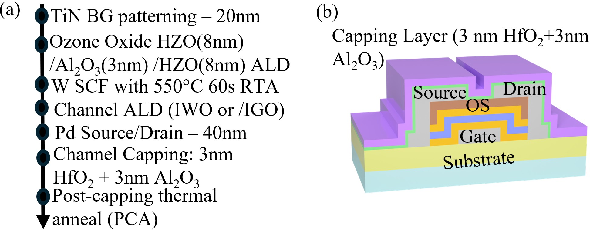
Figure 1: (a) Process flow for back-gated OS-FeFET with channel capping and laminated gate stack; (b) Three-dimensional schematic of capped FeFET device.
Device Fabrication and Methodology
The devices are fabricated using ozone ALD for both the ferroelectric/dielectric gate stack and the capping layers, ensuring high interface quality and precise thickness control. The OS layers are deposited with controlled doping levels to achieve target carrier concentrations and minimize variability. Post-contact, the capping stack is deposited to mitigate oxidation and stabilize the device during subsequent annealing. Annealing is systematically varied (400–650 °C; 10–40 min, N32 ambient), mirroring cumulative 3D-NAND processing conditions.
Impact of Thermal Processing on Electrical Characteristics
The electrical response to PCA is interrogated by DC and pulsed I-V measurements, extracting ON-state current, gate leakage, and state-resolved threshold voltages. The devices endure thermal treatments up to 650 °C for 30 min (IGO) or 10 min (IWO) prior to irreversible channel failure, defined by the complete loss of conduction and V33 extraction.
Thermal stress initially induces a notable positive shift in the erased-state V34 (V35) while leaving the programmed-state V36 (V37) comparatively unchanged, leading to MW enhancement. MW maximizes immediately before the onset of conduction failure. A monotonic decrease in ON-current and degradation in subthreshold swing accompany this shift, linked to increased channel/contact resistance.
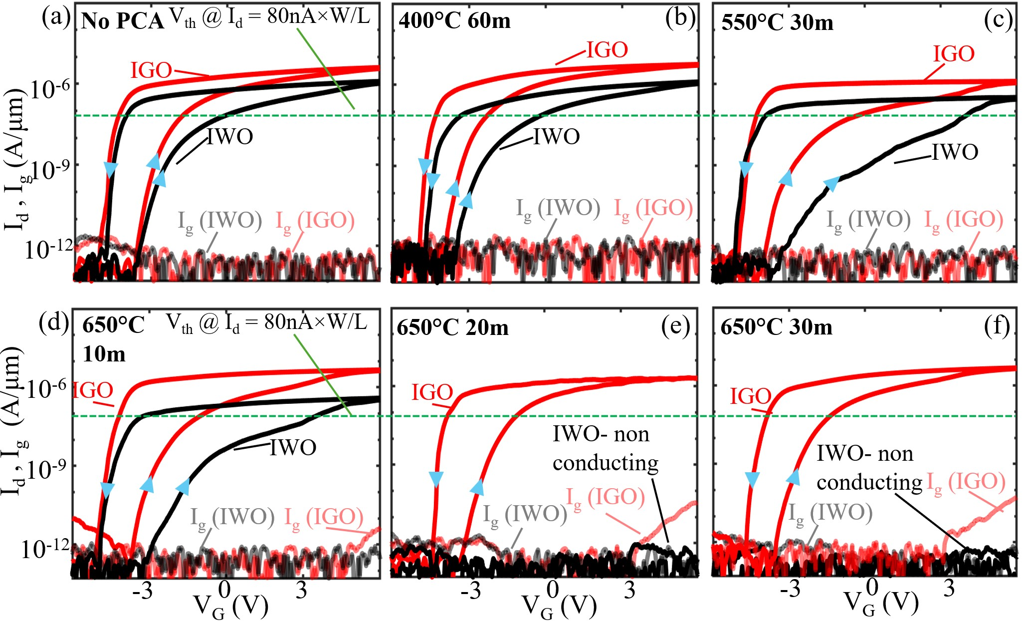
Figure 2: (a) I38-V39 and I20-V21 for pristine devices; (b–c) MW evolution and ON-current degradation after moderate (400–550 °C) PCA; (d–f) Complete channel failure post extended high-temperature annealing.
Quantitative Analysis of Memory Window Evolution
Thermal MW maps, derived from pulsed I-V measurements, highlight the sensitivity of both IWO and IGO channels. For all conditions, IWO exhibits a larger MW relative to IGO, but fails at a lower cumulative thermal budget. The correlation between annealing time/temperature and the MW increase is robust until abrupt catastrophic channel failure, demonstrating that MW improvement is fundamentally limited by oxygen defect dynamics and not ferroelectric stack integrity.
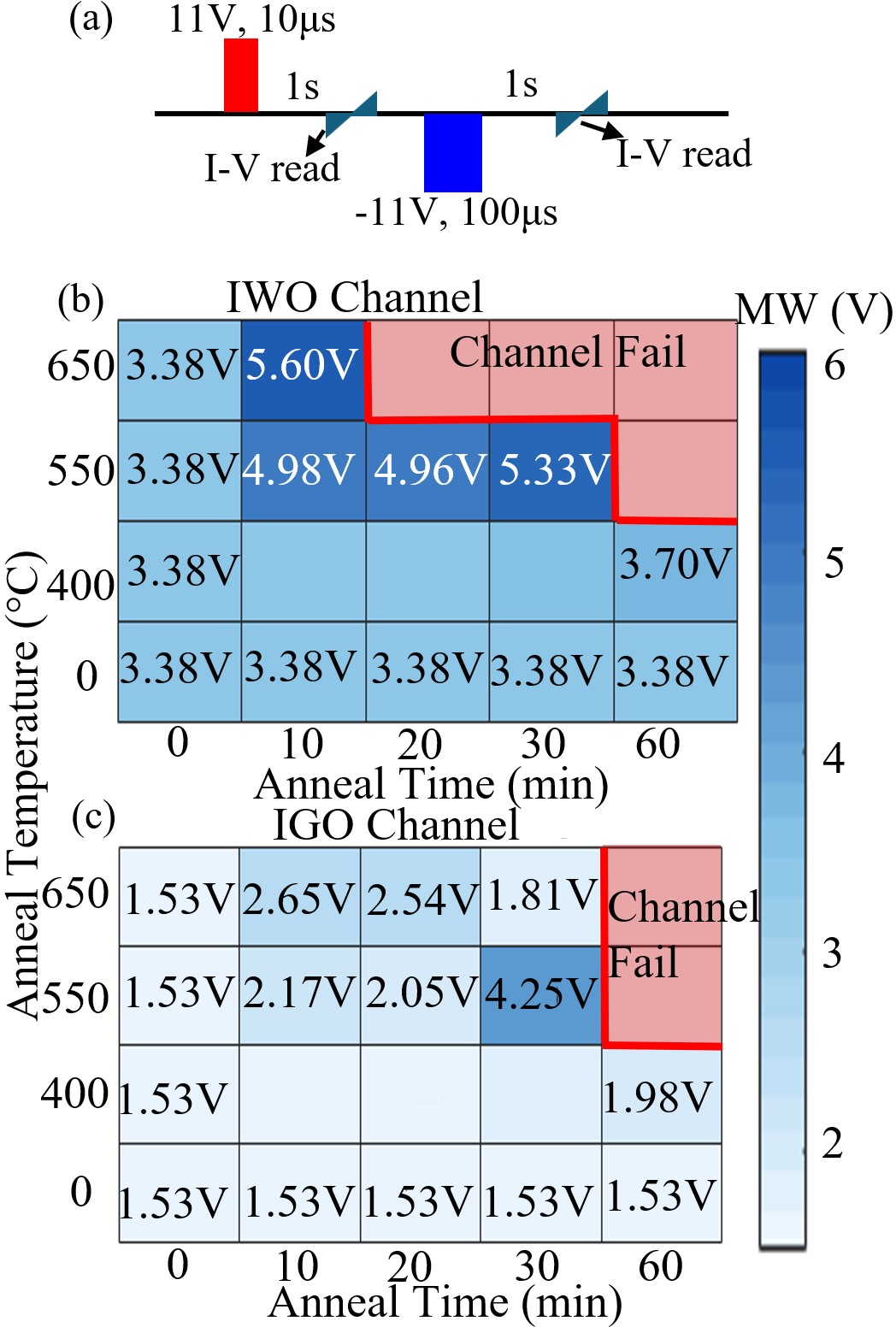
Figure 3: (a) Pulsed I-V MW extraction; (b–c) MW as a function of annealing for IWO and IGO. Peak MW is immediately prior to failure.
The origin of MW maximization is a preferential positive drift in V22, attributed to the increased series resistance and reduced carrier density in the channel post-anneal, a consequence of decreased oxygen vacancy concentration due to O23-V24 recombination.
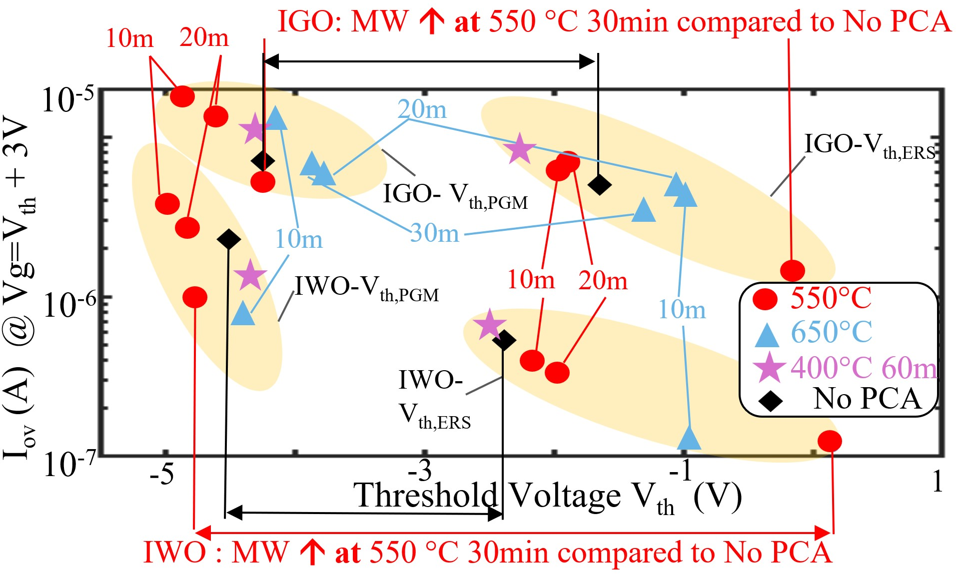
Figure 4: Overdrive current (I25) versus V26 for PGM and ERS states, emphasizing the strong dependence of erased-state shift on thermal budget while ON-state current declines.
Ferroelectric Stack Stability Versus Channel Degradation
MFM capacitor measurements of the gate stack subjected to analogous PCA confirm sustained ferroelectric polarization and minimal change in coercive voltage, even beyond channel failure thresholds. Elevated leakage at maximum anneal is observable yet not dominant; thus, channel transport properties, not ferroelectric degradation, are responsible for device failure.
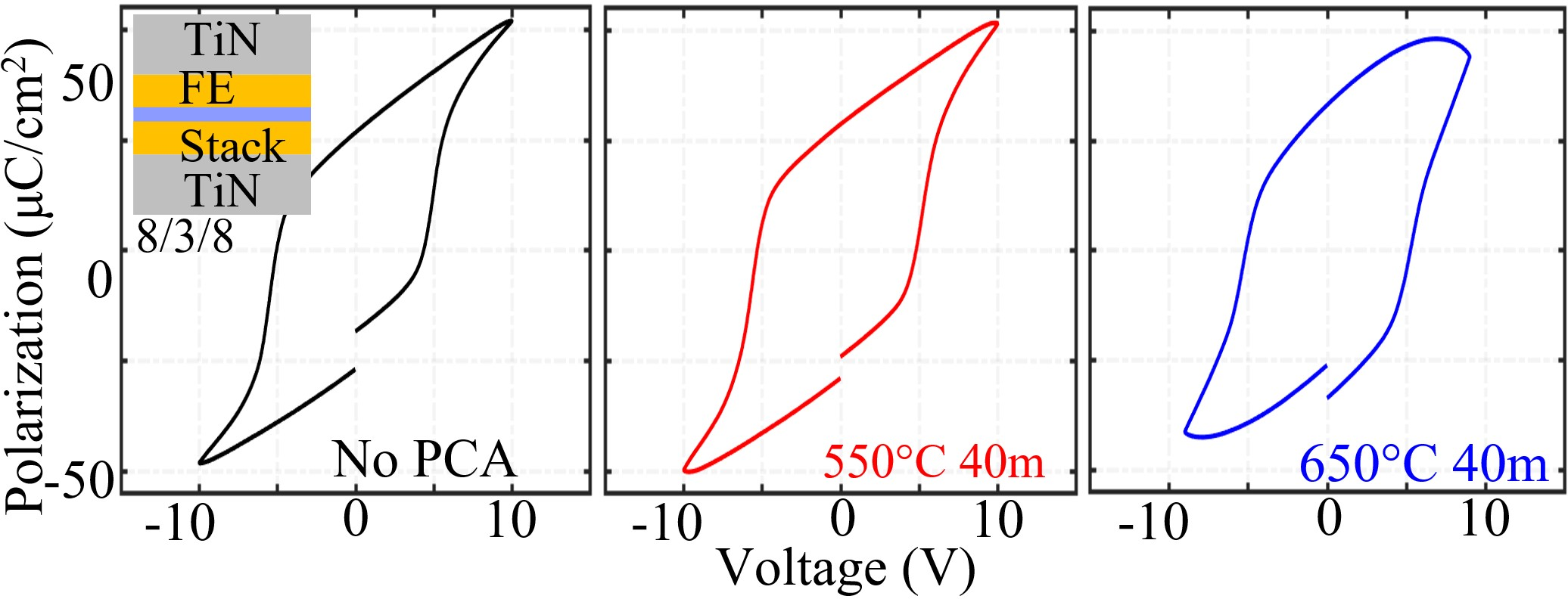
Figure 5: Polarization–voltage (P–V) of MFM structure pre- and post-extreme PCA confirming robust ferroelectric switching.
Structural Mechanism of Channel Failure: Crystallinity and Defect Proximity
GI-XRD offers direct insights into the microstructural evolution induced by PCA. In IWO, a 2.3-fold intensification of the (222) diffraction peak is observed at high annealing, indicating higher crystallinity compared to IGO. The IGO maintains a higher fraction of amorphous phase, increasing the spatial separation between oxygen interstitials and vacancies, and thereby delaying their recombination; IWO’s higher crystallinity facilitates more rapid O27–V28 recombination, leading to faster conduction loss.
The shift of the (440) peak at long annealing times reflects dopant incorporation and lattice contraction, with Ga and W both modulating the structural disorder and functional limits.
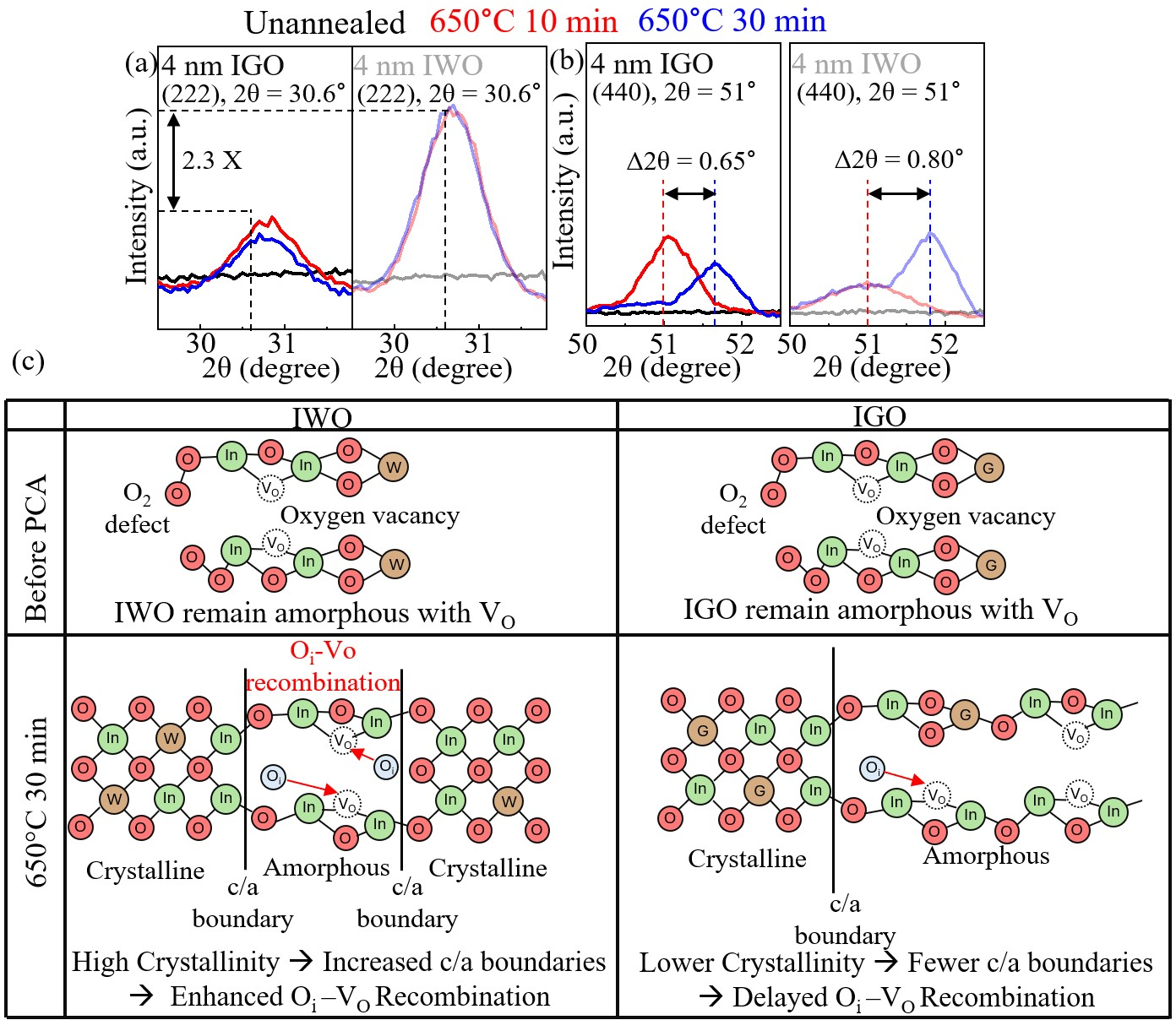
Figure 6: (a) (222) and (b) (440) GI-XRD peaks pre- and post-anneal, (c) Schematic comparison of crystalline/amorphous morphology and defect distributions in IWO vs IGO.
Retention analysis after maximal PCA shows stable state separation for both channel types, underlining that ferroelectric polarization is preserved and that OS-channel defect engineering, not ferroelectric instability, dictates operational boundaries.
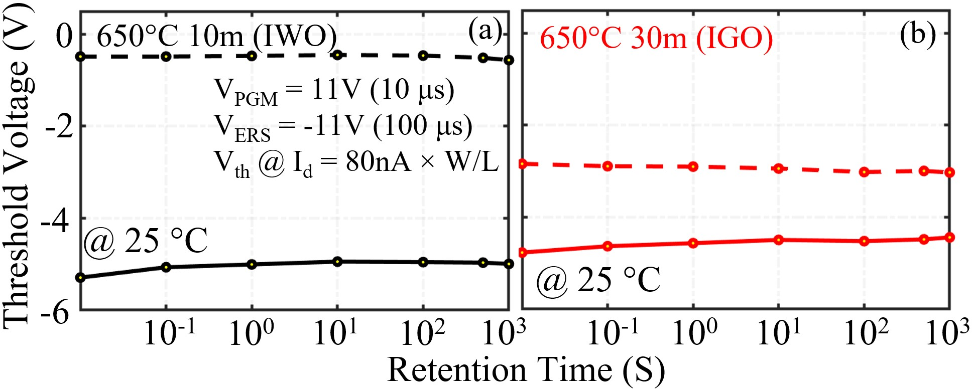
Figure 7: Programmed/erased state retention for IWO (a) and IGO (b) after exposure to respective maximum tolerated thermal budgets.
Implications and Future Directions
The findings reinforce OS-FeFETs as practical for emerging 3D-NAND architectures, provided thermal budgets are tailored to channel composition and defect engineering. The explicit link between MW enhancement and oxygen vacancy annihilation, mediated by channel amorphism/crystallinity, provides actionable guidance for material and process optimization. For applications demanding high MW and data retention at elevated process temperatures, Ga-doped channels with engineered amorphous fraction offer a favorable trade-off. The demonstrated survivability of the ferroelectric stack under aggressive annealing supports the decoupling of ferroelectric and channel degradation, suggesting that subsequent improvements in channel reliability can further advance device integration.
Future advances are expected in compositional and structural channel engineering, such as the introduction of nanolaminates or alloyed oxide semiconductors, to decouple MW from channel degradation and extend operational thermal limits without compromising endurance or retention.
Conclusion
This work establishes clear thermal processing boundaries for oxide-channel FeFETs, quantified by concurrent MW enhancement and conduction failure. The comparative analysis of IGO and IWO demonstrates a strong dependence of thermally induced MW gain and failure mechanisms on channel structure and defect chemistry. Critically, the ferroelectric gate stack remains robust, spotlighting the OS-channel as the limiting component for high-temperature integration. These insights provide a framework for the process optimization of FeFET-based 3D-NAND and next-generation nonvolatile memory.