- The paper introduces an agent-driven framework that automates photonic design using iterative propose–simulate–evaluate loops integrated with multiphysics simulation and design-rule checks.
- It demonstrates significant performance improvements across passive, active, and RF devices, achieving lower losses and optimized electrical routing compared to conventional methods.
- The framework's autonomous hypothesis journaling and layout optimization reduce human error and expedite full-cycle device prototyping, setting a new standard for automated photonic design.
Autonomous Agentic Design for Photonics
Methodology: Agentic Automation Across Multiphysics Design
The paper presents an agent-driven framework for photonic device design, leveraging LLMs as active participants in iterative simulation-driven optimization. Agents autonomously execute experimentation loops (propose–simulate–evaluate–iterate) under explicitly encoded design constraints (fabrication rules, geometric specs, physics checks). The methodology generalizes to arbitrary device classes and simulation modalities—electromagnetic, charge transport, microwave—by interfacing Python-scriptable solvers with agents capable of code generation and reasoning.
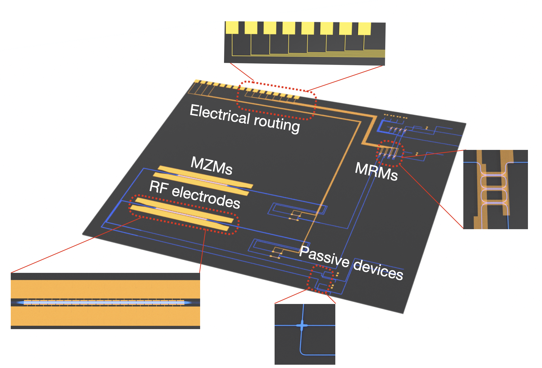
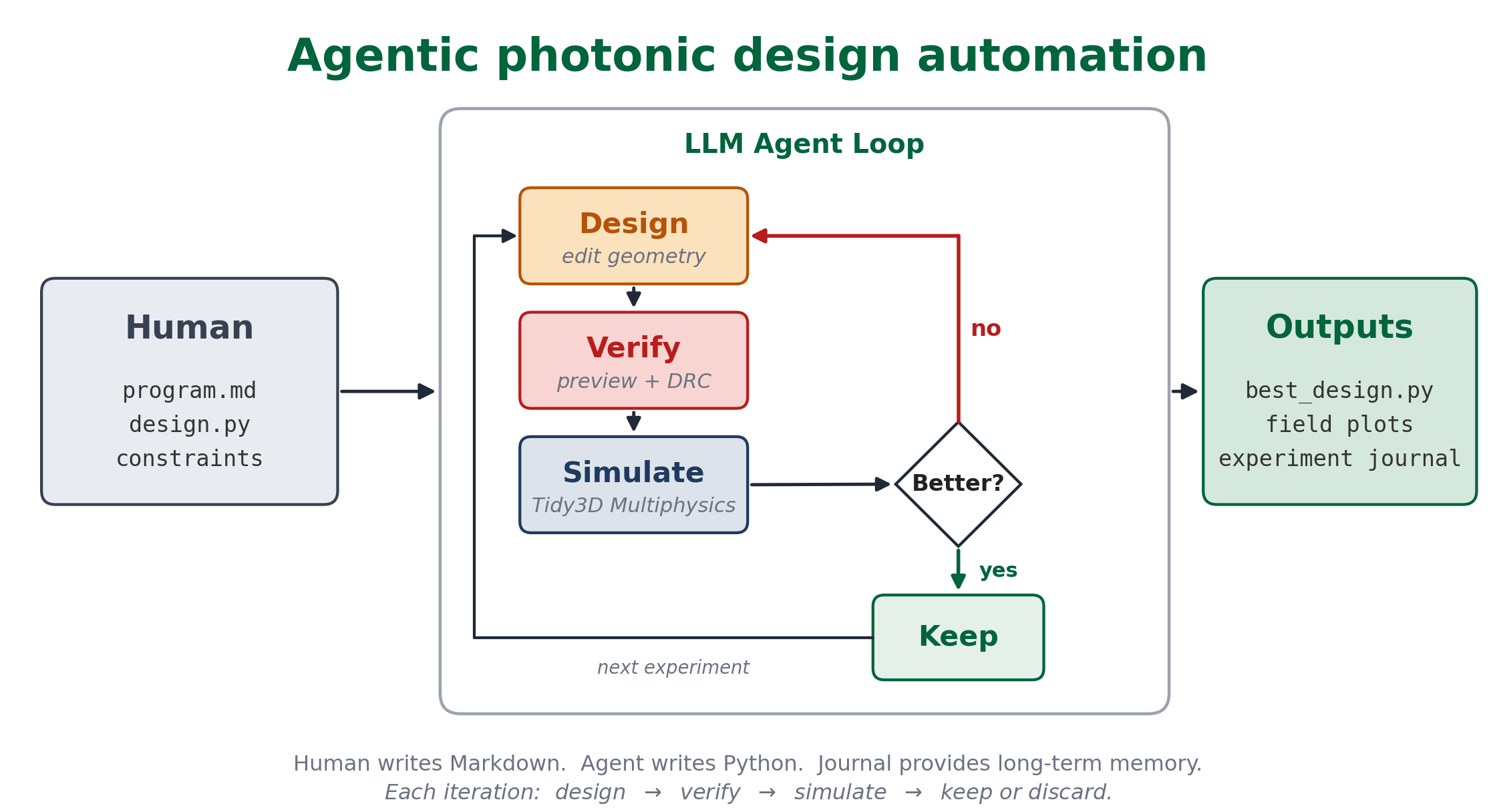
Figure 1: An overview of agentic photonic design automation, highlighting both the chip-level problems addressed (electrical routing, MRMs, passive devices, MZMs, RF electrodes) and the closed verification–simulation–design loop.
Agents receive high-level problem statements, figures of merit, and a suite of simulators, then autonomously generate candidate designs, identify failure modes, and maintain a persistent journal for hypothesis tracking. The approach integrates literature review, hypothesis formation, design-rule checking (DRC), and revision within each loop iteration, ensuring manufacturability and physical plausibility.
Results: Canonical Design Problems
Passive Device Optimization
The agentic loop is demonstrated on fundamental passive photonic components, including SiN bends, SOI splitters, tapers, grating couplers, and crossings. For a compact SiN waveguide bend, the agent achieves 0.109 dB loss at 12 μm radius (97.51% transmission), a 4x reduction vs. the circular baseline (0.460 dB), through sequential introduction of Euler-circular-Euler geometry, width tapering, and inward radial offset. The design innovation mirrors physical intuition: smooth curvature profiles and mode-matched transitions.
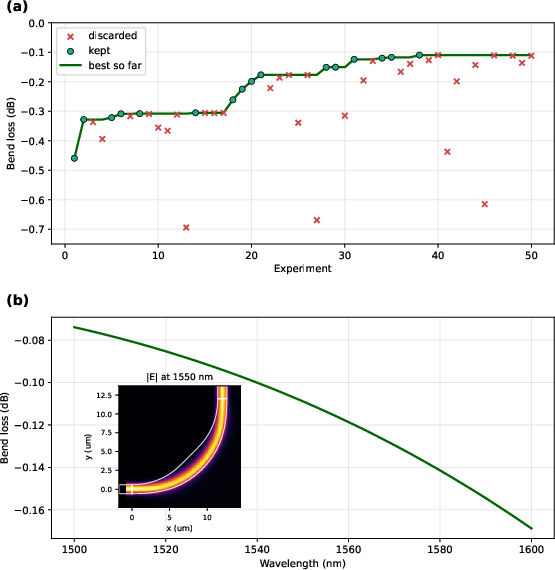
Figure 2: Optimization trajectory of bend loss and wavelength dependence for the SiN passive bend. The agent transitions from discarded candidates to promoted designs, reaching minimal loss.
Performance metrics for other passive classes are similarly competitive: splitter insertion loss at 0.015 dB, taper loss at 0.114 dB, grating coupler loss at 2.89 dB, and crossing loss at 0.11 dB, validating the generalization of the loop.
Active Device Design
For silicon microring modulators (MRMs), the agent couples drift-diffusion charge transport with optical simulation, seeking to minimize the modulation-efficiency product (VπL⋅Cj) without explicit prior on achievable trade-offs. It explores six junction topologies, with the optimal configuration—a U-shaped buried P-island—yielding VπL=0.53 V·cm, Cj=0.83 pF/mm, VπL⋅Cj≈4.4 V·pF. The agent avoids unphysical layouts via generalized DRC, converging on the empirical envelope established in prior literature (Nvidia OFC 2026 compilation).
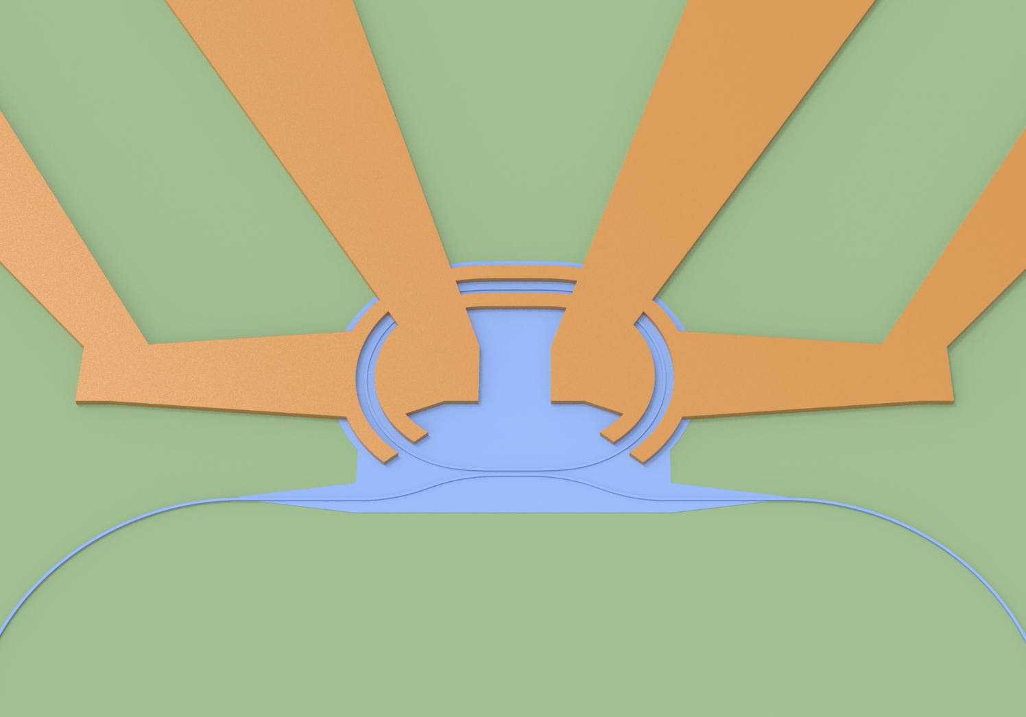
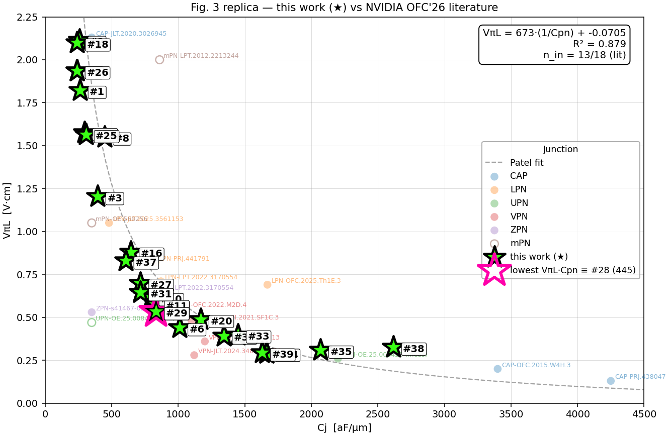
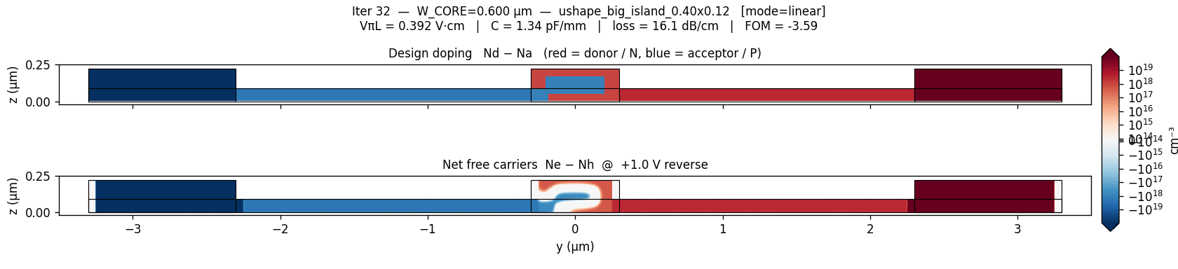
Figure 3: Agentic exploration of the (Cj,VπL) envelope for silicon MRMs, juxtaposed with published benchmarks. The agent traces the trade-off without access to historical devices.
RF Electrode Optimization
For high-speed modulator electrodes, the agent optimizes a multi-parameter, multi-topology transmission line system. The loop cycles through symmetric T-rail, asymmetric T, wide-cap T, T+U, half-T designs, modifying parameters (period, width, gap, metal stack) and pivoting topologies when the journaled evidence indicates stagnation. The best wide-cap T geometry achieves Z0≈43–44Ω and α0≈0.29–0.36 dB·cm−1·GHz−1/2, outperforming the plain T-rail baseline (Z0≈38–41Ω, VπL=0.530).
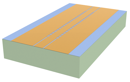
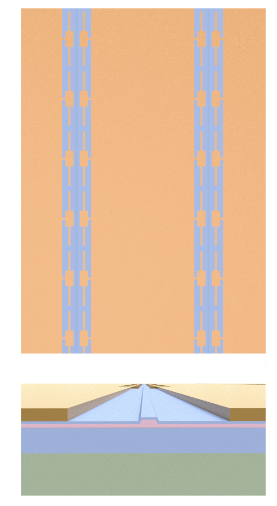
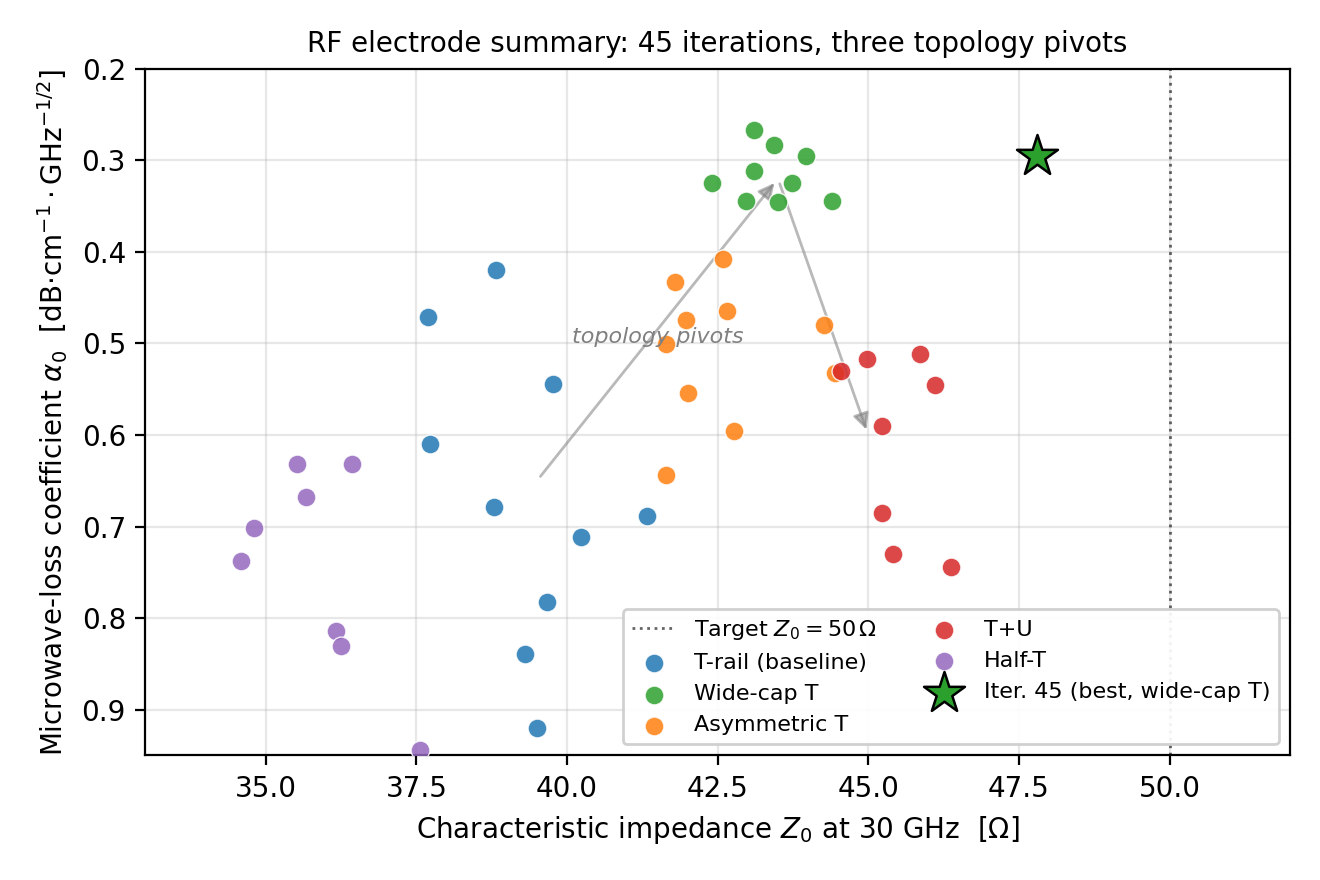
Figure 4: Run trajectory over VπL=0.531 for five electrode topology families, with the wide-cap T achieving the closest match to target specifications.
Chip-Level Electrical Routing
In routing, the agent tackles a combinatorial layout challenge, operating over a grid abstraction and selecting among twelve algorithms. Starting from 192 violations (heater cut-throughs, route crossings), the agent reaches zero violations in 27 iterations (2.5 minutes wall-clock time), leveraging grid planning, obstacle marking, dynamic pin-to-pad assignment, and layout reshaping. The DRC trajectory provides a deterministic optimization signal.
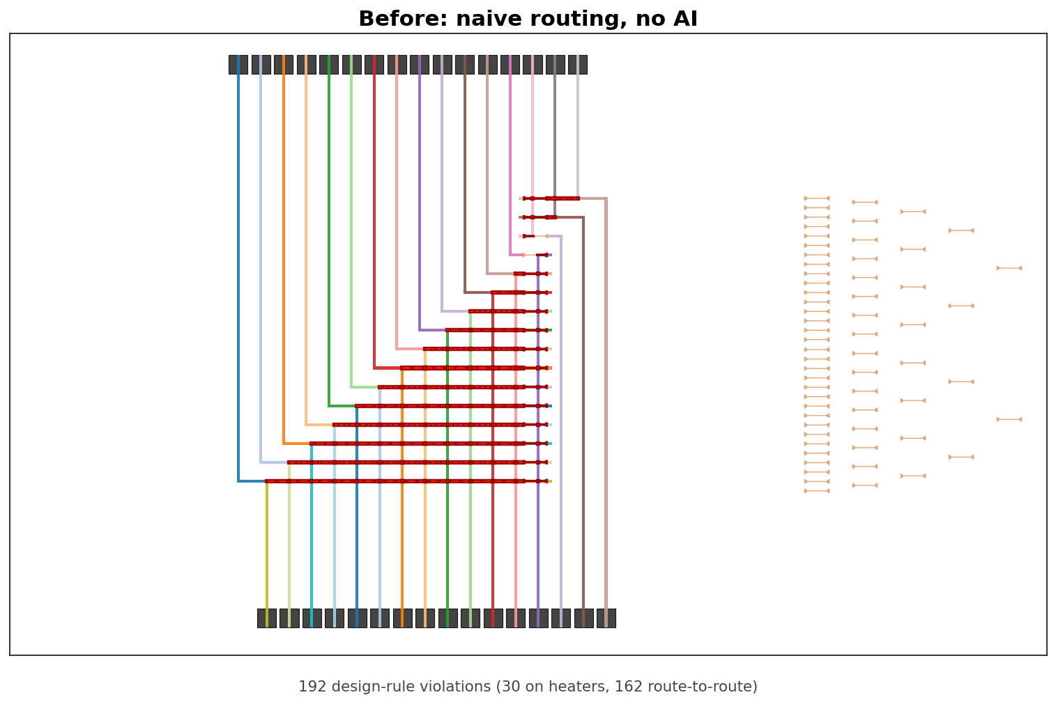
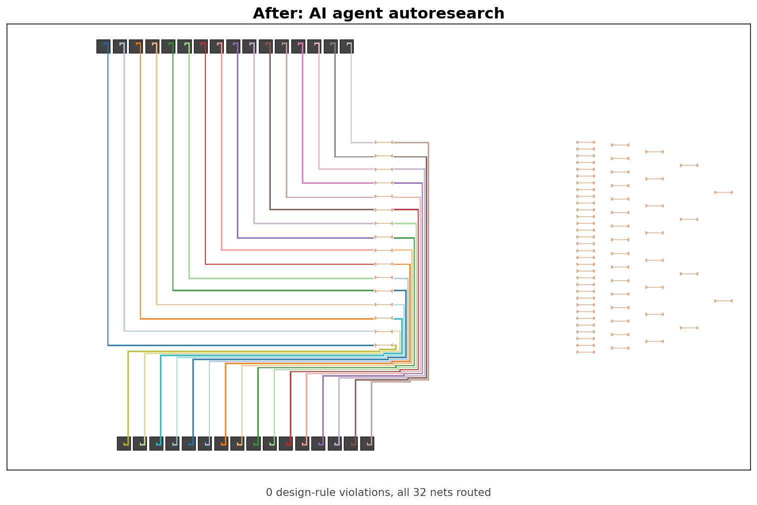
Figure 5: Electrical routing progression, showing the initial layout with 192 DRC violations and the final, violation-free result after agentic optimization.
End-to-End Multiphysics Design: Silicon Mach–Zehnder Modulator
A holistic demonstration combines layout, charge transport, optical mode, and RF simulation in reproducing a published silicon T-rail Mach–Zehnder modulator. Following correction of agent-initialized setup errors (mode misidentification, junction shunt double-count), the agent executes a two-stage optimization loop: (1) sweeping junction doping scaling to populate the VπL=0.532 envelope; (2) Bayesian optimization of the segmented CPS electrode for each selected capacitance, bounded by stringent DRC.
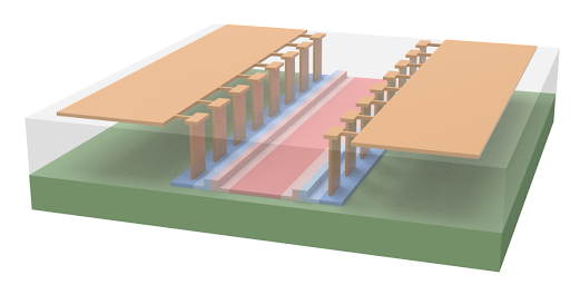
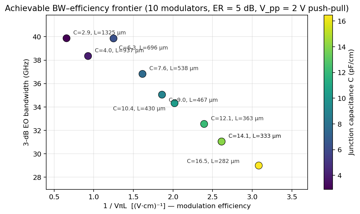
Figure 6: Final 3D rendering of the T-rail modulator and the agentic bandwidth–efficiency frontier, with all designs maintaining VπL=0.533 within VπL=0.53410% of 50 Ω.
The process yields nine distinct devices spanning the bandwidth–efficiency trade-off (29–40 GHz, VπL=0.535 from 0.324–1.523 V·cm). RF metrics (VπL=0.536, microwave loss, VπL=0.537) align closely with expert reference implementations, confirming full-cycle reproduction.
Implications and Future Directions
The demonstrated agent-driven framework sets a new bar for end-to-end autonomous design across photonics subdisciplines: passive, active, RF, and layout. Its architecture is robust to highly coupled multiphysics workflows, discrete parameterization, and combinatorial topology selection. The loop's adaptability, informed by hypothesis journaling and context integration with simulation stacks, enables rapid design cycles and discovery of physical insights absent in black-box optimizers.
Practical implications extend to accelerated device prototyping, reduced human labor, and elimination of repetitive setup errors. Theoretically, agentic loops introduce higher-level reasoning, supporting non-differentiable constraint management, topology pivots, and active debugging of simulation infrastructure. Migration of problem initialization and acceptance criteria into the agent's domain will further decrease reliance on expert supervision.
Integrating fabrication and measurement feedback into the loop would close the gap from simulation to full process validation. Modularization of agents to handle platform-specific process recipes (e.g., TCAD) and device characterization benchmarks is a natural extension for future work, enabling broader generalization to electronic–photonic co-design.
Conclusion
The agent-based photonic design loop is empirically validated across canonical device classes and multiphysics integration, achieving state-of-the-art performance on the leading figures of merit and faithfully reproducing published devices. The loop's autonomy and versatility provide a scalable route to automated design, with foundational implications for both engineering practice and computational design theory.

