- The paper introduces CLIPGen, an automated framework that generates and models chiplet D2D link IP for effective pre-RTL exploration with precise PPA estimates.
- The methodology uses a distributed π-ladder RC channel abstraction, SPICE simulation, and Pareto frontier co-optimization to optimize TX/RX sizing and achieve delay-energy trade-offs.
- Experimental analysis reveals package-driven trade-offs and scalability across multiple process nodes, guiding architectural decisions for advanced 2.5D chiplet SiPs.
CLIPGen: A Chiplet Link IP Modeling and Generation Framework for 2.5D Architecture Exploration
Motivation and Context
The increasing adoption of 2.5D chiplet-based Systems-in-Package (SiPs) has created a demand for architectural frameworks capable of accurate, yet tractable, pre-RTL design-space exploration. Trade-offs in packaging and die-to-die (D2D) link interconnects critically affect system-level power, performance, and area (PPA) metrics. Existing modeling approaches bifurcate into detailed but inflexible models requiring deep packaging expertise, or high-level abstractions lacking sufficient accuracy for architectural decision-making. CLIPGen directly addresses the gap by delivering a configurable, automated, and multi-tech IP generation flow for chiplet D2D links, spanning both early-stage and detailed analysis. Its output artifacts are standard EDA collateral—Liberty, Verilog, LEF—compatible with industry toolchains.
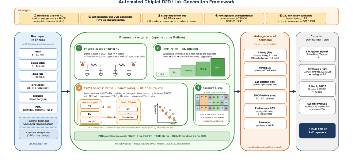
Figure 1: Automated generation flow driven by a single JSON config, yielding channel modeling, link adaptation, TX/RX co-optimization, and area abstraction.
Framework Architecture
CLIPGen operates on the principle of providing realistic power, performance, and area for a parameterized D2D link, abstracting away device- and process-level complexity. Input to the flow is a JSON configuration, encompassing user-facing parameters (package/interposer type, reach, bump pitch, data rate, lane count) as well as optional expert overrides (e.g., coupling capacitance ratios, physical constants). The framework supports two main modes: single-point configuration and design-space sweeps exploring Cartesian products of link parameters.
The modeling workflow initiates with a distributed π-ladder RC channel abstraction, automatically adapted to physical geometry and package technology. Link adaptation then auto-selects termination and passive equalization according to reach and channel loss, fully compliant with UCIe specification boundaries. Transceiver sizing and characterization leverage SPICE simulation via Cadence Liberate, embedding the channel model within the TX subcircuit to yield accurate timing arcs. A Pareto-guided TX/RX co-optimization procedure, based on lookup table interpolation, efficiently finds non-dominated trade-offs in energy and latency over an N×N grid. The resulting IP block area is computed analytically, conforming to bump map and process node constraints.
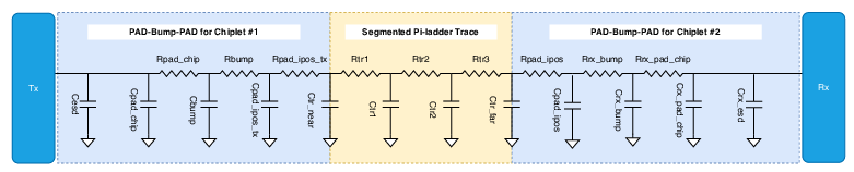
Figure 2: Physical channel model: distributed π-ladder topology with parameterized elements for pads, bumps, trace, and ESD protection.
Channel and Link Modeling Methodology
CLIPGen’s channel model is calibrated for the UCIe standard regime—all relevant RC and geometric parameters are literature-sourced, process-portable, and encapsulated in the hidden config hierarchy. Pad and bump capacitances are derived from parallel-plate and cylindrical models with accurate scaling for bump pitch and package materials. Trace resistance and capacitance are interpolated by width and substrate dielectric. Skin effect and inductive impacts are considered negligible within the specified data rate and reach boundaries.
Termination and equalization are sized automatically by the framework using graduated levels—accommodating reflection suppression requirements beyond unterminated UCIe boundaries and minimizing unnecessary power or area overhead. Passive equalization is implemented as a first-order RC roll-off compensation, avoiding the complexity and power overhead of active feed-forward equalizer implementations.
Transceiver Sizing, Characterization, and Pareto Frontier Construction
The TX architecture follows a tapered CMOS inverter chain, sized via geometric progression and SPICE Q/V characterization to meet UCIe rise/fall targets. Passive equalization elements are patched into the netlist as needed. RX is a two-stage topology balancing minimal input capacitance and core logic drive, parameterized for process and channel geometry.
Joint TX/RX sizing is formulated as a multi-objective optimization. CLIPGen’s approach uses lookup tables and interpolated characterization results, obtaining the Pareto frontier over energy-per-bit and worst-case link latency with only NTX+NRX SPICE runs—highly scalable relative to brute-force grid search. Three canonical operating points—minimum-delay, minimum-energy, and balanced knee—are auto-selected and exposed as collateral.
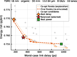
Figure 3: Energy-per-bit vs. worst-case link delay for a 16-lane UCIe standard link, showing the cloud of TX/RX candidate points and the refined Pareto frontier.
Experimental Analysis and Empirical Findings
CLIPGen's design-space exploration reveals nuanced and, in some cases, counter-intuitive package trade-offs. In a comparative sweep of short-reach links (2–25 mm) at 48 Gb/s, the energy and delay curves for organic substrates and silicon interposers cross over—organic packages outperform silicon beyond ~10 mm reach in energy efficiency, with >2× margin at 25 mm despite silicon’s smaller bump capacitance (organic: 0.41 pJ/bit vs. silicon: 0.83 pJ/bit at TSMC 16nm for best-power selection). Silicon retains a modest latency advantage only at 2–4.5 mm, after which channel resistance drives delay higher.
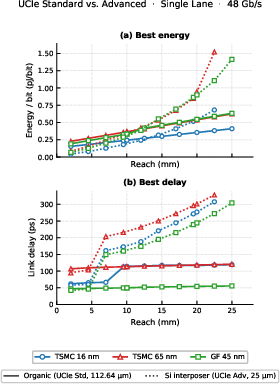
Figure 4: Single-lane 48 Gb/s link energy and delay comparison for organic vs. silicon substrates; crossover observed near 10 mm for energy efficiency.
Multi-lane reach sweeps across TSMC 16nm, TSMC 65nm, and GF 45nm nodes at 48 Gb/s show clear separation—TSMC 16nm exhibits the lowest energy per bit (∼0.77 pJ/bit at 30 mm), GF 45nm achieves minimum delay (∼60 ps at 30 mm), and TSMC 65nm represents a balanced trade-off. These results directly inform architectural decisions on package and node selection, highlighting the super-linear growth of channel RC at longer reaches and its impact on required driver stage count and link feasibility.
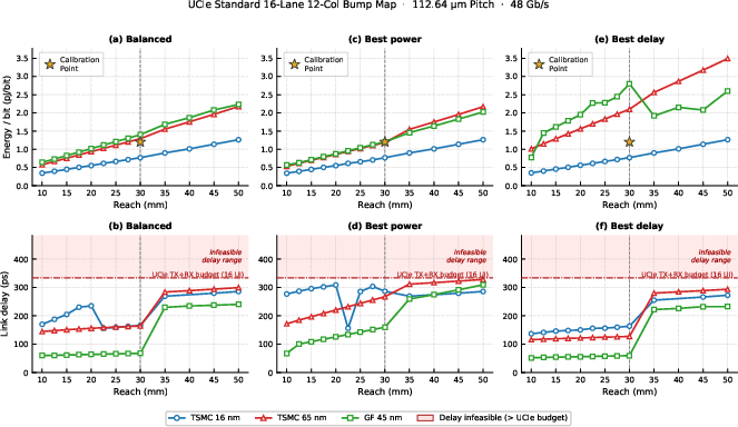
Figure 5: Modeled energy-per-bit and worst-case link delay vs. reach (2–50 mm) for 16-lane chiplet links across three process nodes, three optimal design-point selectors.
Implications and Future Directions
The practical implications of CLIPGen are significant for architectural design, IP block integration, and package selection in chiplet-based SiPs. The ability to rapidly and accurately evaluate PPA trade-offs—including package-driven phenomena not captured by high-level models—enables system-level co-optimization without deep packaging expertise. The framework’s modularity and multi-PDK support facilitate porting to emerging process nodes, and its output collateral integrates seamlessly with industry workflows.
Theoretically, CLIPGen’s distributed channel modeling and Pareto-guided co-optimization extend the scope of architectural exploration. By embedding physical parameterization and accurate cross-coupled sizing into early-stage analysis, it bridges modeling fidelity with practical usability, addressing a longstanding gap noted in prior work on chiplet interface modeling [Arch-LUCIE-MICRO, Arch-interface-Micro23].
Future research directions include extending CLIPGen to higher data rates where inductive effects and skin effect substantially impact signal integrity, as well as supporting advanced 3D chiplet stacking architectures with corresponding thermal, RC, and electromagnetic modeling. Integration with cost and yield models [feng2022chiplet, graening2023chiplets] and multi-fidelity thermal analysis [pfromm2025mfit, zhou2022thermal] will further mature the framework’s holistic system-level impact.
Conclusion
CLIPGen provides a robust, automated pipeline for chiplet D2D link IP modeling, directly embedding channel RC into SPICE-level characterization for realistic Liberty timing arcs. Its modular design, multi-PDK support, and automated adaptation mechanisms enable rapid exploration of PPA, revealing critical package-level trade-offs and informing architectural design. The framework fills a key void in pre-RTL analysis, making accurate interconnect modeling accessible to system architects and directly facilitating cross-package, cross-node optimization (2605.27757).

