A Wafer-Scale Heterogeneous III-V-on-Silicon Nitride Quantum Photonic Platform
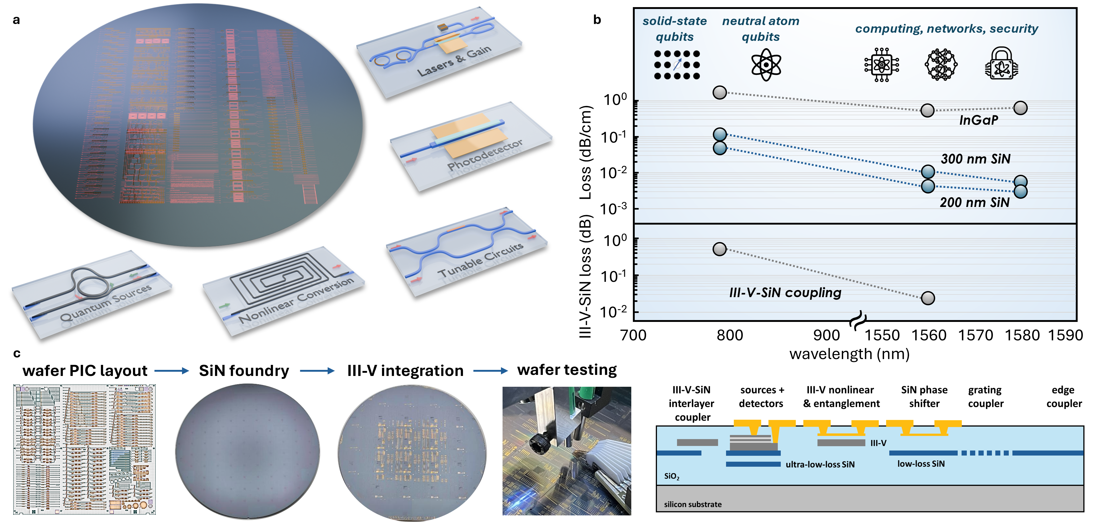
Abstract: Heterogeneous integration of gain and strongly nonlinear materials with ultra-low-loss silicon nitride (SiN) photonics offers a route to scalable quantum circuits, but concurrent wafer-scale manufacturability, low interlayer loss, and high performance have been challenging to realize. Here we demonstrate a wafer-scale III-V-on-SiN quantum photonic platform that directly integrates III-V layers to foundry-fabricated SiN circuits. The SiN layer provides 200-300 nm thick waveguides with $<1$ dB/m loss and a mature passive photonics ecosystem, while III-V materials provide large $χ{\left(2\right)}$ and $χ{\left(3\right)}$ nonlinearities for parametric gain, frequency conversion and quantum light generation. Adiabatic interlayer couplers yield $<25$ mdB loss to InGaP waveguides and resonators with intrinsic quality factors exceeding $106$, enabling $15\times$ brighter entanglement sources and efficient nonlinear conversion on SiN. Integrated components--including low-loss beam splitters, waveguide crossers, and tunable interferometers--are complemented by III-V lasers and InP photodetectors with amplifiers achieving up to $99{+1}_{-12}\%$ quantum efficiency and $3$ GHz bandwidth. This architecture unites ultra-efficient sources, nonlinear elements and detectors on a wafer-scale, low-loss platform, establishing a path toward large-scale, low-noise quantum photonic systems.
Paper Prompts
Sign up for free to create and run prompts on this paper using GPT-5.
Top Community Prompts
Explain it Like I'm 14
What is this paper about?
This paper shows how to build “light circuits” for quantum technology on a single, mass-producible chip. The team combines two kinds of materials:
- Silicon nitride (SiN): great for making ultra‑low‑loss “roads” that guide light very far with almost no energy lost.
- III‑V semiconductors (like InGaP and InP): great for making lasers, detectors, and special “tricks” that let light change color or create pairs of entangled photons.
By sticking (bonding) these materials together across an entire wafer (a big, pizza‑sized slice of semiconductor), they make chips that include bright quantum light sources, powerful light converters, precise tunable circuits, and near‑perfect detectors—all on one platform that can be manufactured at scale.
What questions were they trying to answer?
The researchers focused on three simple goals:
- Can we make a chip that combines the best “roads” for light (SiN) with the best “devices” (III‑V lasers, converters, and detectors) at wafer scale, so we can build lots of identical, high‑quality chips?
- Can we move light between the layers (from SiN to III‑V and back) with almost no loss, so the different parts work together efficiently?
- Can this platform generate, manipulate, and measure quantum light (like entangled photon pairs or squeezed light) with much better performance than before?
How did they do it? (With easy analogies)
Think of a city designed for light instead of cars:
- SiN waveguides are ultra‑smooth highways for light, with very little “friction” (loss). They’re great for long, stable routes.
- III‑V layers are like power plants and funhouses: they supply energy (lasers and amplifiers) and can bend or “repaint” light (nonlinear effects) to new colors or states useful for quantum tasks.
To connect these two, they built very gentle ramps (adiabatic couplers) so light can move from one layer to another without “bumping” and losing energy.
Key parts of their approach:
- Wafer‑scale bonding: They attach large III‑V sheets onto already‑made SiN circuits, so many chips can be made at once, like baking many cookies from one big tray.
- Resonators (tiny racetracks for light): These make light circle around many times, boosting interactions so effects like color‑doubling (second‑harmonic generation, SHG) and pair creation (spontaneous parametric down‑conversion, SPDC) become very efficient.
- Tunable filters and interferometers: These act like adjustable traffic lights and bridges to route and control light precisely.
- Clever photodetectors: They designed detectors where light bounces around inside the absorbing material (like a tiny mirrored room), so almost every photon gets caught, achieving near‑perfect efficiency.
Whenever a technical term appears:
- Nonlinearity (χ(2), χ(3)): A material property that lets light beams interact—like one beam changing the color of another or splitting a high‑energy photon into two lower‑energy “twin” photons.
- SHG (second‑harmonic generation): Turning a photon of one color into a photon of exactly double frequency (like 1560 nm → 780 nm).
- SPDC: Splitting a higher‑energy photon into two lower‑energy, correlated photons—often used to make entangled pairs.
What did they find, and why is it important?
They achieved several best‑in‑class results, all on the same platform:
- Extremely low‑loss light highways (SiN): Less than 1 dB of loss per meter—very low for on‑chip optics—so signals stay strong and clean.
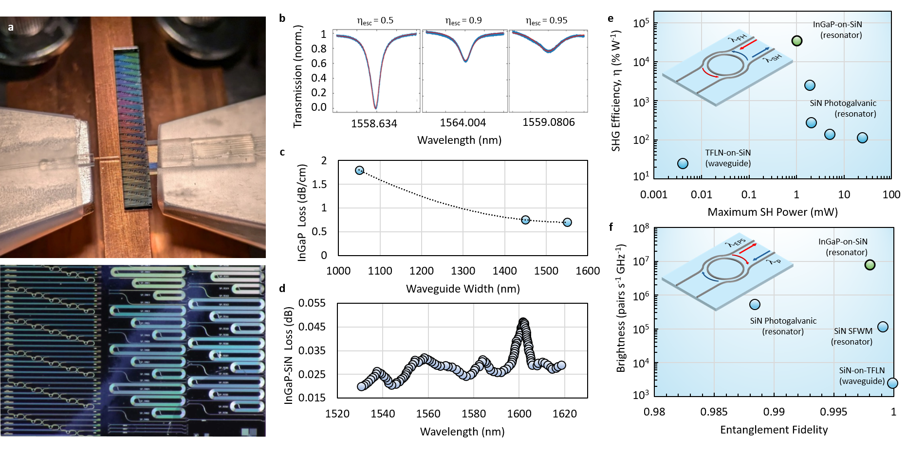
- Super‑efficient layer “ramps”: Moving light between SiN and InGaP lost less than ~0.025 dB (over 99% makes it through), which is excellent for combining functions.
- High‑quality InGaP resonators: With intrinsic quality factors above 1,000,000, meaning light circles many times, boosting nonlinear effects.
- Record‑level color conversion on SiN: Resonators achieved SHG efficiencies above 35,000% per watt, the highest reported on SiN to their knowledge.
- Much brighter entangled‑photon sources: About 15× brighter than previous SiN‑based sources, while keeping very high entanglement quality.
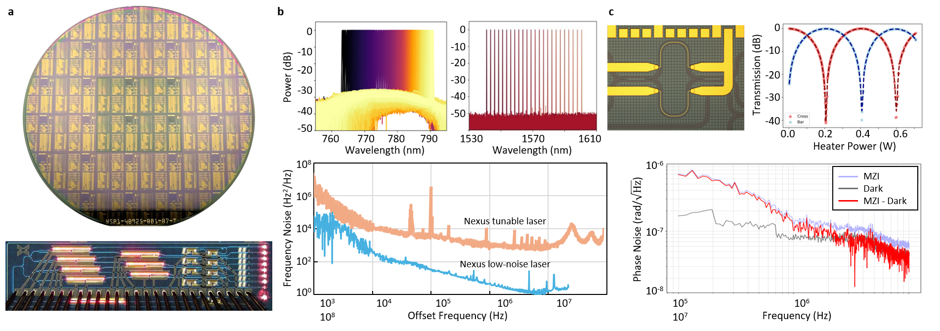
- Integrated, tunable, low‑noise lasers: Operated at both 1560 nm (telecom) and 780 nm (near‑visible), with very narrow linewidths (down to hertz‑level when stabilized), which is crucial for precise quantum measurements.
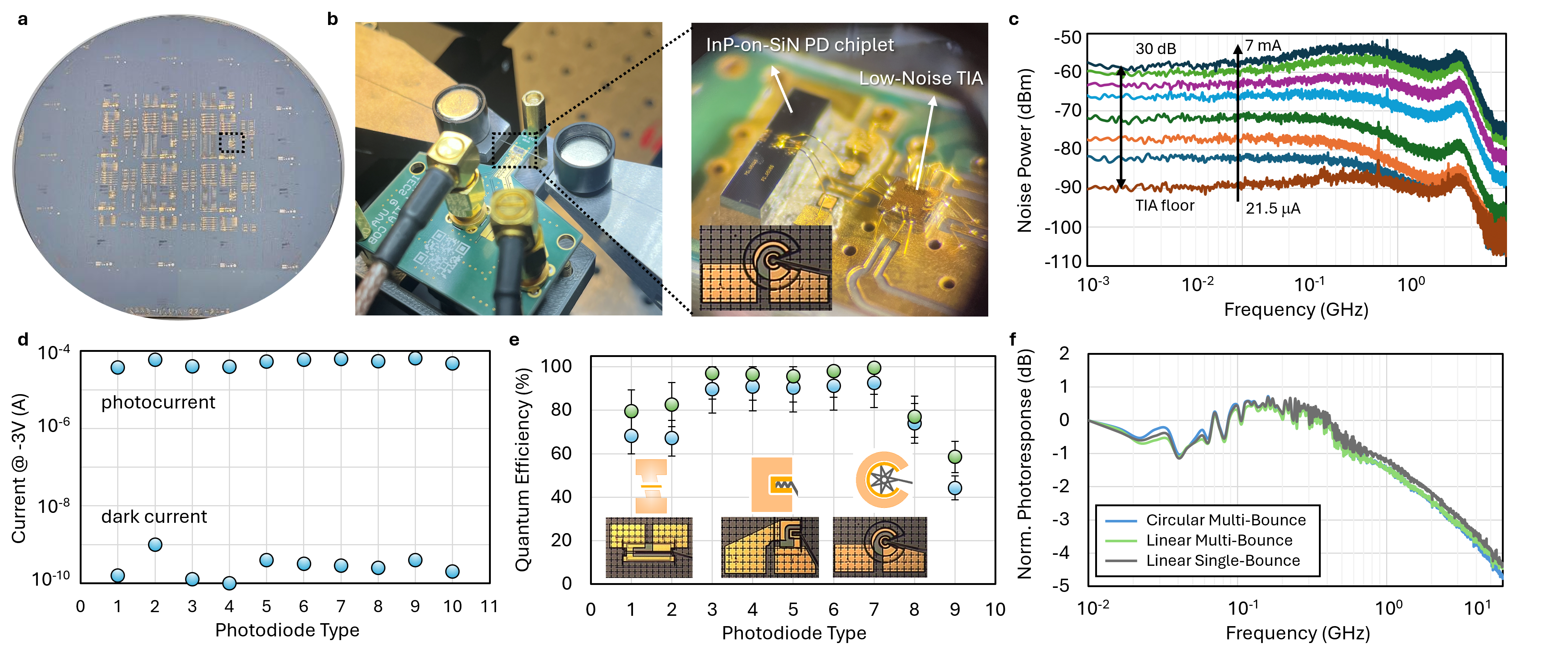
- Near‑unity‑efficiency photodetectors: Quantum efficiency up to about 99% with fast response (hundreds of MHz to GHz), and very low electronic noise—ideal for detecting delicate quantum signals like squeezed light.
- Stable, low‑loss interferometers: With tiny insertion loss and high extinction ratios, plus very low phase noise for stable measurements.
Why it matters: Quantum photonic systems need all three pillars—great sources, great circuits, and great detectors—working together with minimal loss and noise. This platform brings them together on a wafer‑scale, manufacturable chip, which is a big step toward practical quantum technologies.
What could this lead to?
This work lays the groundwork for compact, mass‑producible quantum photonic devices that could:
- Power secure quantum communications by creating and routing entangled photons efficiently.
- Improve ultra‑precise sensors (like those used to detect tiny motions or fields) through squeezed light and low‑noise readout.
- Help scale up quantum computing and networking by offering bright, clean, and controllable on‑chip light sources, with built‑in lasers and detectors.
In short, the team shows a path to building “quantum labs on a chip,” where light can be generated, transformed, routed, and measured—all with very low loss and noise—using a process that can make many high‑quality chips at once. This combination of performance and manufacturability is key to turning quantum photonics from lab demos into real‑world technology.
Knowledge Gaps
Knowledge gaps, limitations, and open questions
Below is a concise, actionable list of the main gaps and unresolved questions left by the paper, organized by topic to aid follow-on research and engineering.
Wafer-scale fabrication, yield, and reliability
- Wafer-scale yield and variability are not quantified (e.g., distributions of layer-to-layer coupling loss, waveguide loss, Q factors, detector QE, laser performance) across wafers/lots; provide statistical process control data and lot-to-lot reproducibility.
- Direct-bonding reliability under thermal cycling, humidity, and long-term operation is unreported; perform accelerated aging and environmental stress tests for InGaP–SiN and InP–SiN interfaces.
- Co-integration of both GaAs-based (780 nm) and InP-based (C-band) epitaxies on the same wafer is asserted but not demonstrated; detail process compatibility, bonding order, and cross-contamination/thermal budget constraints.
- Post-III–V-processing impact on the ultra-low-loss SiN waveguides is only stated qualitatively (“no significant impact”); quantify pre-/post-bonding SiN loss and resonator Q changes with confidence intervals.
Interlayer coupling and polarization management
- 780 nm interlayer couplers have ~0.5 dB loss; required design/process steps to achieve <0.1 dB (e.g., thicker SiN, smaller taper tips, improved lithography/etch) are not developed or validated.
- Tolerance, bandwidth, temperature dependence, and back-reflection of the TE (C-band) and TM (780 nm) interlayer couplers are not reported; characterize polarization selectivity, fabrication sensitivity, and reflection-induced laser noise.
- No on-chip polarization conversion/management is shown despite reliance on mixed TE/TM operation; demonstrate robust polarization rotators/splitters and quantify polarization drift over time/temperature.
Nonlinear sources and frequency conversion
- SPDC source performance focuses on brightness and CAR; spectral purity, indistinguishability, and Schmidt number are not measured; perform joint spectral intensity/phase measurements and heralded-g2(0) to quantify single-mode operation.
- Pump–resonator stabilization and drift management (especially for resonant 780 nm pumping) are not demonstrated; implement and characterize on-chip resonance locking and long-term stability under varying thermal loads.
- High-Q SHG resonators show “saturation at lower power” without analysis of mechanisms (e.g., photothermal effects, thermal bistability, free-carrier or defect-related absorption); quantify thermal dynamics, stability ranges, and damage thresholds.
- Modal phase-matching in InGaP is used, but dispersion engineering bandwidth, temperature tunability, and fabrication tolerances for SHG/SPDC are not analyzed; provide design rules for robust phase matching across device/process variations.
- Claims of “quantum frequency conversion” are not experimentally supported; demonstrate difference-frequency/sum-frequency conversion with efficiency, noise figure, and fidelity metrics.
- Internal loss and escape efficiency of the prospective OPO (for squeezing) in InGaP resonators are not characterized; measure intrinsic/extrinsic Q, coupling conditions, and parametric oscillation thresholds on the integrated platform.
Integrated lasers and amplifiers
- Actual laser relative intensity noise (RIN) and frequency noise spectra over the relevant bands for squeezing and homodyne detection are not reported; measure RIN vs. frequency, quantify sensitivity to on-chip reflections, and compare to the model assumptions.
- Robustness and lock-acquisition dynamics of self-injection locking to ultra-high-Q resonators under environmental perturbations are not shown; characterize lock stability, re-lock behavior, and sensitivity to thermal/mechanical noise.
- Thermal tuning (Vernier filters, heaters) is the only control demonstrated; assess power consumption, thermal cross-talk in dense circuits, and long-term drift; explore fast, low-power tuning (electro-optic or piezoelectric) options.
- ASE and gain ripple from on-chip SOAs and their impact on quantum components (e.g., increased background in detectors or sources) are not quantified; measure ASE spectra and implement/assess integrated filtering and isolation strategies.
- Integrated optical isolation is absent; evaluate strategies to suppress back-reflections (e.g., angled interfaces, anti-reflection engineering, nonreciprocal or time-varying isolators) and quantify their effect on laser noise and circuit performance.
Linear photonic components and circuits
- Only MZI metrics are provided; performance of other claimed components (beam splitters, waveguide crossers, filters) is not quantified; report insertion loss, imbalance, cross-talk, and phase stability for each element.
- MZI phase noise is reported from 100 kHz–10 MHz; low-frequency (<100 kHz) stability critical to quantum interferometry is uncharacterized; measure drift over seconds–hours and demonstrate integrated feedback/locking for long-term operation.
- Scaling behavior for large interferometric meshes (thermal cross-talk, calibration overhead, heater count and power) is not addressed; provide design and control strategies for large programmable circuits.
Photodetectors and homodyne receivers
- The bandwidth is inconsistently described (3 GHz in abstract vs. 510 MHz 3 dB for the co-packaged receiver); clarify detector-only vs. TIA-limited bandwidth, and provide modulation response/linearity up to multi-GHz with CMRR vs. frequency.
- Near-unity QE is reported with large asymmetric uncertainty (99{+1}_{-12}%); reduce calibration uncertainty (e.g., absolute power metrology, integrated power monitors) and report wafer-scale QE statistics.
- Dynamic range, saturation current/voltage, linearity, and recovery times under high photocurrent (e.g., >10 mA) are not presented; map linear operation regions for homodyne and classical readout use cases.
- Temperature dependence of QE, dark current, and noise is not reported; characterize performance across operating temperatures and under thermal loads from nearby heaters/lasers.
- Extension of the detector concept to 780 nm (or other bands) is suggested but not demonstrated; fabricate and characterize visible-band detectors (material choice, absorption enhancement, QE, noise).
- System-level CMRR is 50.4 dB at 10 MHz without active balancing; quantify CMRR across frequency and under practical LO power imbalance, and demonstrate on-chip active balancing to maintain >60 dB over the target band.
System-level quantum demonstrations and noise budgets
- The squeezed-light “transceiver” is conceptual; no on-chip squeezing is demonstrated; realize and measure on-chip SHG+OPO squeezing, reporting internal loss, escape efficiency, and observed squeezing vs. model predictions.
- The squeezing model excludes several likely degradations (e.g., OPO cavity internal loss, phase noise from thermal cross-talk, scattering-induced stray light); extend the noise budget to include these and validate experimentally.
- Stray light management (especially at 780 nm) and its impact on on-chip detectors and quantum states is not addressed; design and quantify on-chip pump rejection, dump structures, and scatter suppression.
- Integration of single-photon detectors (e.g., SNSPDs) on the same platform is not explored; assess cryo-compatibility, back-end process integration, and optical/electrical co-design for hybrid classical/quantum detection.
- Packaging for large-scale systems (fiber arrays, hermetic sealing, thermal management, EMI shielding) and its impact on phase/noise performance is not discussed; develop and benchmark scalable packaging strategies.
Performance at additional wavelengths and applications
- Operation is shown at 780 nm and 1550 nm; applicability to other key quantum wavelengths (e.g., 637 nm NV centers, 795/852 nm atomic lines, 1064 nm) is untested; demonstrate material stacks and dispersion/coupler designs for these bands.
- Coherent frequency links between disparate systems (e.g., visible–telecom conversion) are proposed but not realized; implement and benchmark conversion fidelity and noise for heterogeneous quantum network interfaces.
Modeling, metrology, and reproducibility
- Provide first-principles models linking fabrication tolerances (thickness, width, bonding gap) to interlayer coupling, dispersion, and phase-matching bandwidth, validated by across-wafer measurements.
- Measurement methods for entanglement fidelity rely on CAR as a proxy; perform full state tomography or Bell tests to rigorously quantify fidelity and purity at target brightness levels.
- Report comprehensive uncertainty budgets for all key metrics (loss, QE, linewidths, brightness, SHG efficiency), and publish open datasets to enable independent verification and benchmarking.
Practical Applications
Overview
This paper presents a wafer-scale heterogeneous III–V-on-silicon nitride (SiN) quantum photonic platform that co-integrates:
- Ultra-low-loss SiN waveguides (<1 dB/m) and high-Q (Q > 106) resonators,
- III–V nonlinear materials (InGaP) for highly efficient χ(2)/χ(3) processes (e.g., SHG and SPDC),
- Integrated III–V active devices (InP/GaAs) for tunable lasers and optical gain,
- Near-unity-quantum-efficiency InP-on-SiN photodiodes with low-noise TIAs,
- Low-loss interferometric circuits (e.g., MZIs) with high extinction and low phase noise.
Below are concrete, real-world applications derived from the platform’s demonstrated capabilities. Each item lists target sectors, example tools/products/workflows, and key dependencies/assumptions.
Immediate Applications
The following can be deployed now or with modest engineering for lab/industrial prototypes, based on the demonstrated device performance.
- Bright, fiber-compatible entangled-photon pair sources at 1550 nm (academia, telecom/quantum networking)
- What: Wafer-scale SPDC microresonator sources with >15× brightness vs. native SiN, ~108 pairs s-1 GHz-1 (normalized to 10 µW pump), CAR > 104, and 99.9% two-photon entanglement fidelity at 106 pairs/s.
- Tools/products/workflows: Packaged chip modules with fiber I/O; external SNSPDs for detection; 780 nm on-chip or external pumps using the integrated lasers/SHG.
- Dependencies/assumptions: Efficient fiber-chip coupling; thermal stabilization; use of off-chip single-photon detectors (SNSPDs) for counting; pump-laser stability.
- High-efficiency on-chip second-harmonic generation modules (test & measurement, atomic physics, metrology, telecom)
- What: InGaP-on-SiN resonator-based SHG with >35,000 %/W efficiency (state-of-the-art on SiN), enabling compact frequency doublers (e.g., 1560→780 nm) for rubidium spectroscopy, optical frequency references, and laboratory instrumentation.
- Tools/products/workflows: Co-packaged 1560 nm integrated tunable lasers + resonator SHG; thermal tuning for doubly resonant operation; fiber-pigtailed modules.
- Dependencies/assumptions: Thermal control to maintain resonance; power handling and photothermal/photorefraction management; packaging to minimize coupling loss.
- Narrow-linewidth, tunable integrated lasers for coherent sensing and metrology (telecom/datacom test equipment, LiDAR seeding, precision metrology)
- What: 1560 nm and 780 nm III–V-on-SiN lasers with kHz-level free-running linewidths; hertz-level with self-injection locking to ultra-high-Q SiN resonators; >10 mW output; >40–50 dB SMSR; ≥60 nm tuning at 1560 nm and ≥25 nm at 780 nm.
- Tools/products/workflows: Self-injection-locked laser modules; compact frequency references; seed lasers for FMCW LiDAR or interferometric sensors.
- Dependencies/assumptions: Access to ultra-high-Q resonators for injection locking; environmental isolation; long-term frequency stabilization loops as needed.
- Near-unity-quantum-efficiency balanced photoreceivers for homodyne detection (quantum sensing, CV-QKD testbeds, coherent optical instrumentation)
- What: InP-on-SiN photodiodes with up to 99% QE (bounded), low dark current (<1 nA), and a co-packaged 510 MHz TIA achieving >30 dB shot-noise clearance (10 MHz–>1 GHz) and ~50 dB CMRR at 10 MHz.
- Tools/products/workflows: Turnkey balanced homodyne receivers for squeezed-light detection and CV-QKD prototyping; coherent receiver front-ends for lab instruments.
- Dependencies/assumptions: Local oscillator (LO) power/relative intensity noise within modeled bounds; thermal management; alignment and matching of detector pairs.
- Ultra-low-loss, low-noise interferometric circuits for coherent routing and phase control (quantum labs, classical coherent systems)
- What: SiN MZIs with <6 mdB insertion loss, >40 dB extinction, and <0.4 mrad RMS phase noise (100 kHz–10 MHz) for precise interferometric operations.
- Tools/products/workflows: Reconfigurable routing networks; tunable beam splitters; phase shifters for homodyne angle control and multi-path quantum circuits.
- Dependencies/assumptions: Heater calibration and thermal crosstalk management; integration with control electronics for long-term stability.
- Heterogeneously integrated III–V gain and power distribution on SiN (complex photonic subsystems in R&D and pilot production)
- What: On-chip seed laser feeding multiple SOAs with integrated monitor photodiodes for scalable power distribution and dynamic signal management.
- Tools/products/workflows: Multi-channel amplified photonic engines for experiments requiring multiple pumps/LOs; wafer-scale testing and binning.
- Dependencies/assumptions: Thermal control for gain sections; device matching across die/wafer; reliability testing for continuous-wave operation.
- Wafer-scale prototyping and foundry workflows for heterogeneous quantum PICs (semiconductor manufacturing, academia, startups)
- What: Design–fabricate–test flow for 200 mm SiN wafers with back-end III–V bonding, adiabatic interlayer couplers (<0.05 dB C-band loss), and integrated testing.
- Tools/products/workflows: PDKs including III–V-on-SiN building blocks (lasers, SHG, SPDC, detectors, MZIs); chiplet-based integration; wafer-level parametric test.
- Dependencies/assumptions: Access to the bonding and back-end flow; yield and uniformity across wafers; maturing design kits and process control.
- Standards and benchmarking inputs for quantum photonics (policy/standards bodies, consortia)
- What: Empirical reference points for loss (<1 dB/m), QE (~99%), coupling (<0.05 dB), laser linewidths (Hz–kHz), and entanglement source brightness/fidelity to inform component standards and procurement specs.
- Tools/products/workflows: Contribution to interoperability requirements, metrology protocols, and qualification metrics (e.g., Telcordia-like for quantum PICs).
- Dependencies/assumptions: Community coordination; round-robin measurements; shared data sets.
- Workforce development and education (academia, training programs)
- What: Hands-on labs using packaged III–V-on-SiN quantum PICs to teach integrated quantum photonics, nonlinear optics, and coherent detection.
- Tools/products/workflows: Standardized teaching modules; MPW runs for student designs; open reference designs for lasers/SHG/SPDC/detectors.
- Dependencies/assumptions: Affordable access to MPW/foundry; robust packaging; curriculum integration.
Long-Term Applications
These require additional R&D, scaling, or productization (e.g., higher levels of integration, bandwidth, or reliability).
- Fully integrated quantum photonic transceivers for squeezed-light sensing and CV-QKD (quantum communications, precision sensing)
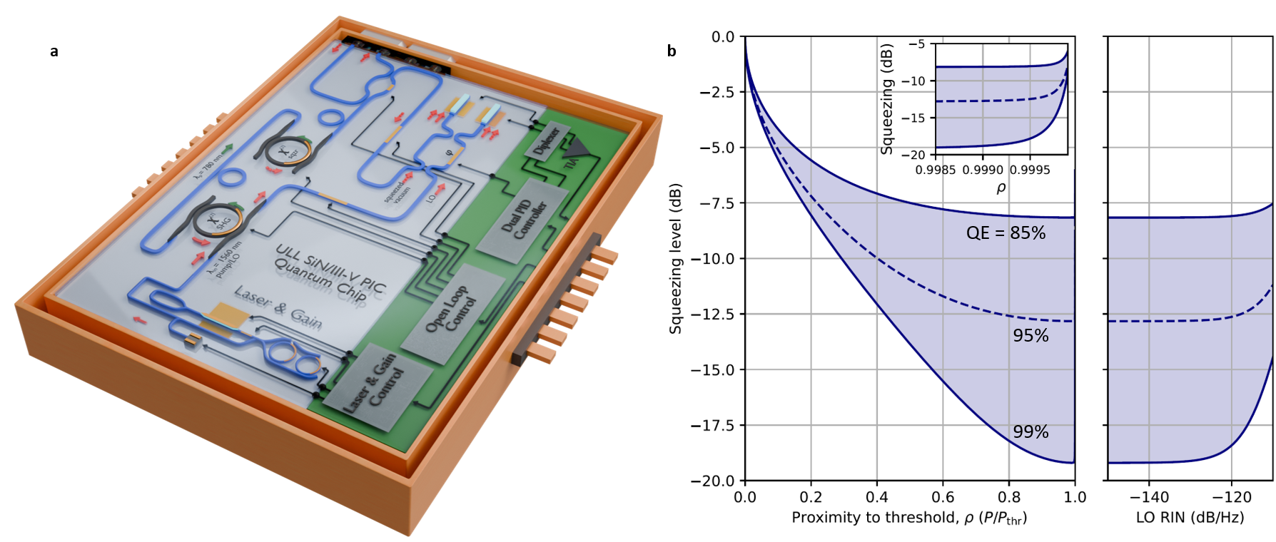
- What: On-chip lasers, SHG/OPO squeezing stages, MZIs, and near-unity-QE balanced homodyne in one package for compact, phase-stable transceivers. Modeling indicates detection limited primarily by photodiode QE for high CMRR and low LO RIN.
- Potential products/workflows: Co-packaged photonics–electronics modules for CV-QKD links and squeezed-light-enhanced sensors (e.g., interferometric readouts).
- Dependencies/assumptions: On-chip OPO realization and stabilization; feedback control and thermal management; rugged packaging; low-RIN lasers in deployed environments.
- Large-scale continuous-variable (CV) quantum processors and cluster-state generation (quantum computing)
- What: Arrays of on-chip squeezed states routed by ultra-low-loss interferometers with high-fidelity detection for scalable CV quantum computing primitives.
- Potential products/workflows: Multi-channel squeezed-light generators; reconfigurable interferometric meshes; integrated detection arrays and control ASICs.
- Dependencies/assumptions: Further reduction of loss and phase noise across large meshes; high-yield, repeatable tuning; integrated electronics for real-time feedback and error mitigation.
- Quantum frequency conversion interfaces across disparate qubit platforms (quantum networking, hybrid systems)
- What: III–V χ(2) devices on SiN to bridge visible/near-IR emitters (e.g., trapped ions, Rb/Cs, NV/SnV centers) to the telecom C-band for low-loss fiber networking.
- Potential products/workflows: Chip-scale quantum transducers (DFG/SFG/QFC) co-packaged with sources/detectors; wavelength-translation modules for quantum repeater nodes.
- Dependencies/assumptions: Demonstration of low-noise, high-efficiency single-photon frequency conversion; integration with single-photon detectors (SNSPDs) or coupling to them with minimal loss; pump-rejection and filtering.
- Coherent optical communications modules with ultra-low phase-noise PICs (telecom/datacenter)
- What: Heterogeneous lasers and near-unity-QE photodiodes for coherent transceivers with lower power and footprint; potential on-chip filters for LO cleanup.
- Potential products/workflows: Co-packaged optics with integrated lasers, SOAs, and detectors; DSP-friendly coherent receiver front-ends.
- Dependencies/assumptions: Telcordia-grade reliability; scaling detector/TIA bandwidth from 0.5–3 GHz to tens of GHz for >100 Gbaud systems; CMOS co-integration; thermal and shock robustness.
- Integrated FMCW LiDAR engines and precision metrology units (automotive/robotics, industrial sensing)
- What: Hertz-level seed lasers and low-loss interferometers on SiN for long-coherence FMCW ranging; on-chip frequency conversion for visible/near-IR operation.
- Potential products/workflows: Compact, low-SWaP LiDAR seeds; frequency-agile reference sources; integrated beamforming with low-loss MZIs.
- Dependencies/assumptions: High-speed phase/frequency modulation (likely via co-integration with LN or Si modulators); power scaling; environmental hardening.
- Fieldable quantum-enhanced sensors (defense, geoscience, space, healthcare R&D)
- What: Squeezed-light-enhanced interferometric sensors (e.g., gravimetry, magnetometry, precision displacement) enabled by compact, robust PICs.
- Potential products/workflows: Ruggedized modules for airborne/spaceborne platforms; OCT-like instruments exploring quantum noise reduction in lab-to-field transitions.
- Dependencies/assumptions: Demonstrated stable squeezing at application-relevant frequencies and conditions; radiation hardness and thermal cycling reliability; domain-specific safety/medical approvals.
- Standardized heterogeneous quantum PIC foundry ecosystem (policy, industry infrastructure)
- What: Mature PDKs, MPW runs, design rules, and qualification procedures for III–V-on-SiN quantum PICs, enabling supply-chain scaling and interoperability.
- Potential products/workflows: Turnkey design kits with verified cells (lasers, SHG/SPDC blocks, detectors, MZIs); automated test suites; yield/performance dashboards.
- Dependencies/assumptions: Sustained investment in process control, bonding yield, interlayer coupling uniformity, and packaging standards; community-driven benchmarks.
- Hybrid integration with additional nonlinear/gain materials (materials/devices)
- What: Co-integration of thin-film LN, AlGaAs, or emerging materials with III–V-on-SiN for broader wavelength coverage, EO modulation, and enhanced χ(2)/χ(3) toolsets.
- Potential products/workflows: Multi-material stacks combining strong EO modulation, high-efficiency frequency conversion, and low-loss routing.
- Dependencies/assumptions: Multi-material bonding compatibility; thermal budget management; interlayer coupling designs across more layers; process complexity control.
Notes on Cross-Cutting Assumptions and Dependencies
- Packaging and coupling: Achieving low total insertion loss requires robust fiber/pigtail attachment and mode-matched interfaces. Interlayer couplers are <0.05 dB at 1550 nm, but fiber-chip loss and package-induced drift must be managed.
- Thermal and phase stability: Many functions (e.g., resonant SHG, injection-locked lasers, MZIs) rely on thermal tuning and stable phases; closed-loop controls and low-drift packaging are important.
- Detector modality: Near-unity-QE photodiodes enable homodyne/heterodyne detection; single-photon counting still requires SNSPDs or SPADs (not integrated here).
- Bandwidth targets: Demonstrated photoreceiver bandwidth is ~510 MHz (with platform capability to multi-GHz); telecom transceivers and LiDAR will require higher-speed modulators/detectors and co-integration with EO materials.
- Reliability and qualification: Transition to products (especially in telecom/automotive/space/medical) will require Telcordia-like reliability, radiation tolerance (space/defense), and compliance testing.
- Foundry access and yield: Widespread adoption depends on availability of MPW runs, mature PDKs, and wafer-scale yield for both SiN and heterogeneous III–V processes.
Glossary
- nonlinearity: Second-order optical nonlinearity enabling processes like SHG and SPDC. "III-V materials provide large and nonlinearities for parametric gain, frequency conversion and quantum light generation."
- nonlinearity: Third-order optical nonlinearity used for Kerr effects and parametric processes. "III-V materials provide large and nonlinearities for parametric gain, frequency conversion and quantum light generation."
- adiabatic interlayer coupler: A gradual mode-conversion structure that transfers light between layers with minimal loss. "Adiabatic interlayer couplers yield ~mdB loss to InGaP waveguides and resonators with intrinsic quality factors exceeding "
- add-drop microresonator: A resonant cavity with separate add and drop ports for filtering or photon-pair extraction. "Add-drop InGaP microresonators are also designed for entangled-photon pair generation via SPDC."
- anti-squeezed quadrature: The noise-amplified quadrature in a squeezed state orthogonal to the squeezed quadrature. "Phase noise degrades the measured squeezing level by partially projecting the anti-squeezed quadrature onto the squeezed quadrature"
- balanced homodyne detector: A detection scheme using differential measurement with a strong LO to read optical quadratures. "An integrated balanced homodyne detector was constructed with a differential balanced pair of circular multi-bounce photodiodes and a custom low-noise transimpedance amplifier (TIA)"
- butt-coupled: Directly joining waveguide facets so light passes straight into another medium/device. "and then butt-coupled into the III-V absorber region."
- CMOS foundry: A semiconductor manufacturing facility/process node used for large-scale photonic wafer fabrication. "originally fabricated at the 200-mm CMOS foundry scale"
- coincidence-to-accidental ratio (CAR): A metric for pair-source quality comparing true to accidental coincidences. "the coincidence-to-accidental ratio (CAR), which is used to estimate the entanglement fidelity."
- common-mode rejection ratio (CMRR): Measure of how well differential systems suppress common signals/noise. "which sets an upper bound on the common-mode rejection ratio (CMRR) of ~dB"
- continuous-variable cluster states: Large, multipartite entangled states used for CV quantum computing. "continuous-variable cluster states for quantum computing"
- cut-back measurements: A method to extract propagation loss by comparing transmissions of different lengths. "Likewise, at 780~nm loss cut-back measurements demonstrate waveguide propagation losses of 8~dB/cm."
- direct bandgap: A semiconductor band structure allowing efficient radiative recombination for gain/lasers. "combining direct bandgap gain media with some of the largest and nonlinearities"
- direct bonded: A wafer-bonding method that joins materials without adhesives for low-loss interfaces. "InGaP is direct bonded through an established process"
- diplexer: A network that separates or combines different frequency bands on a single port. "including an integrated diplexer to separate the buffered squeezed light detection signal and the MZI angle control signal."
- epitaxy: Layered crystal growth of semiconductors providing tailored gain/absorption properties. "enabled by InP-based epitaxy for 1560 nm and GaAs-based epitaxy for 780 nm"
- escape efficiency: Fraction of resonator-circulating photons that couple out into the bus waveguide. "escape efficiencies of 0.5, 0.9, and 0.95"
- evanescently coupled: Coupling via overlapping evanescent fields between adjacent waveguides. "Light propagating in the SiN waveguide is first evanescently coupled into an intermediary dielectric waveguide"
- free spectral ranges (FSR): The frequency spacing between consecutive resonances of a cavity. "Two microring resonators with slightly detuned free spectral ranges form a compact, thermally tunable filter mirror"
- heterogeneous integration: Combining dissimilar materials/devices on one chip for complementary functionality. "Heterogeneous integration of gain and strongly nonlinear materials with ultra-low-loss silicon nitride (SiN) photonics offers a route to scalable quantum circuits"
- high-Q microresonators: Compact cavities with high quality factor for enhanced nonlinear/laser performance. "High-Q InGaP microresonators, low-loss tunable SiN components, and integrated III-V lasers and photodetectors"
- InGaP: Indium gallium phosphide, a III–V semiconductor with wide bandgap and strong nonlinearities. "Among them, InGaP is particularly attractive due to its wide bandgap, absence of two-photon absorption at telecommunications wavelengths, and ability to support sub dB-cm waveguides"
- InP: Indium phosphide, a III–V semiconductor widely used for telecom lasers and photodiodes. "InP photodetectors with amplifiers achieving up to ~\% quantum efficiency and $3$~GHz bandwidth."
- integrating-sphere detector: A detector using multiple internal reflections to increase absorption probability. "effectively forming an integrated analog of an optical integrating-sphere detector."
- intrinsic quality factors: Resonator Q limited only by internal losses, excluding coupling losses. "resonators with intrinsic quality factors exceeding "
- inverse tapers: Tapered waveguide sections narrowing to transfer mode confinement between layers. "Adiabatic inverse tapers are designed for efficiently transferring C-band fundamental transverse electric (TE) modes between the two layers."
- local oscillator (LO): A strong coherent reference beam used in homodyne/heterodyne detection. "local oscillator (LO) relative intensity noise (RIN) with CMRR = ~dB."
- Mach-Zehnder interferometer (MZI): A two-arm interferometer for phase control and coherent routing. "In addition to active light sources, we also realize SiN Mach-Zehnder interferometers (MZIs) integrated on the same platform"
- mdB (millidecibel): A thousandth of a decibel; used to specify very small insertion/coupling losses. "Integrated Mach Zehnder interferometer with ~mdB insertion loss, ~dB extinction, and ~mrad interferometric phase noise"
- modal phase matching: Aligning effective indices/modes to satisfy momentum conservation for nonlinear processes. "which is required to achieve modal phase matching for the SPDC and SHG processes in the waveguides and resonators"
- optical parametric oscillation threshold: Pump level at which an OPO begins to oscillate. "proximity to the optical parametric oscillation threshold, given as the ratio of the in-waveguide pump power over the threshold power."
- parametric gain: Amplification arising from nonlinear interactions driven by a pump. "provide large and nonlinearities for parametric gain, frequency conversion and quantum light generation."
- PECVD: Plasma-enhanced chemical vapor deposition, a thin-film deposition technique. "followed by PECVD cladding and metallization for thermal tuning."
- photogalvanic-poled: A method to induce effective nonlinear response in SiN via photogalvanic poling. "photogalvanic-poled SiN"
- photonic integrated circuits (PICs): On-chip optical circuits integrating multiple photonic components. "ultra-low-loss SiN photonic integrated circuits (PICs)"
- pulley coupler: A coupling geometry where a bus waveguide wraps partially around a resonator for tailored coupling. "Representative microresonator transmission spectra near 1560 nm for resonators designed for escape efficiencies of 0.5, 0.9, and 0.95 (left-to-right)."
- quantum frequency converters: Devices that shift photon frequency while preserving quantum state. "quantum frequency converters on a common wafer-scale platform."
- relative-intensity noise (RIN): Fluctuations in laser intensity, expressed as a spectral density. "local oscillator (LO) relative intensity noise (RIN) with CMRR = ~dB."
- self-injection locking: Stabilizing a laser by feeding back light from a high-Q resonator to narrow linewidth. "laser frequency noise is further suppressed via self-injection locking to ultra-high-Q SiN resonators"
- second harmonic generation (SHG): Nonlinear process converting photons at frequency ω into 2ω. "second harmonic generation (SHG)"
- semiconductor optical amplifiers (SOAs): Semiconductor devices that provide optical gain on-chip. "semiconductor optical amplifiers (SOAs), and monitor photodiodes co-integrated with passive circuitry"
- shot noise clearance: The margin by which measured noise exceeds the shot-noise floor. "Shot noise clearance measurements were taken up to 7~mA of photocurrent where \textgreater30 dB of shot noise clearance is seen from 10~MHz to \textgreater1 GHz."
- silicon nitride (SiN): A low-loss dielectric waveguide material used for photonic circuits. "Silicon nitride (SiN) integrated photonics has emerged as a leading platform for quantum technologies"
- spontaneous parametric down conversion (SPDC): A nonlinear process generating correlated photon pairs at lower frequency. "spontaneous parametric down conversion (SPDC)"
- thin film lithium niobate (TFLN): A high-χ(2) material in thin-film form for efficient nonlinear optics. "thin film lithium niobate (TFLN)-on-SiN"
- transimpedance amplifier (TIA): An amplifier converting photocurrent to voltage with defined gain. "A key feature of this platform is the photodetector coupling and absorption strategy... and a custom low-noise transimpedance amplifier (TIA)"
- transverse electric (TE) modes: Waveguide modes with electric field predominantly transverse to the propagation direction. "Measured III-V-to-SiN adiabatic transition losses for 1550 nm TE modes"
- transverse magnetic (TM) modes: Waveguide modes with magnetic field predominantly transverse to the propagation direction. "Adiabatic inverse tapers are also designed in the same InGaP-SiN layer for coupling 780~nm fundamental transverse magnetic (TM) modes"
- two-photon absorption: Simultaneous absorption of two photons, often a loss mechanism at high intensities. "absence of two-photon absorption at telecommunications wavelengths"
- ultra-high-Q resonators: Resonators with extremely high quality factors enabling hertz-level laser linewidths. "self-injection locking to ultra-high-Q SiN resonators implemented here in a multilayer SiN architecture"
- Vernier ring resonator filters: Paired resonators with slightly different FSRs creating a narrow, tunable passband. "Tunable semiconductor lasers operating at 1560 nm and 780 nm are implemented based on wavelength-selective SiN Vernier ring resonator filters embedded within extended laser cavities."
- wafer-scale: Pertaining to fabrication or integration across an entire semiconductor wafer. "Here we demonstrate a wafer-scale III-V-on-SiN quantum photonic platform"
Collections
Sign up for free to add this paper to one or more collections.

