- The paper demonstrates that RF reflectometry in large-area SiC MOSFETs relies on resistive variations in the drift region rather than on traditional gate-channel capacitance.
- It employs a comprehensive circuit model and numerical simulations to analyze the impact of parasitic capacitance and carrier freeze-out on device sensitivity.
- A modified PCB design incorporating additional inductive and capacitive elements is proposed to redirect RF current, restoring sensitivity under cryogenic conditions.
Gate-Based Radio-Frequency Reflectometry in Silicon Carbide Vertical MOSFETs
Introduction and Motivation
The work investigates the feasibility and limitations of radio-frequency (RF) reflectometry readout in vertical, large-area silicon carbide (SiC) MOSFETs. RF reflectometry is widely utilized for high-bandwidth charge sensing in nanoscale quantum devices but is rarely applied to devices with substantial parasitic capacitance, which are typical of scalable, cryogenic CMOS environments. The study addresses a critical scaling roadblock: how large device geometries and associated parasitics degrade reflectometry sensitivity, and how this challenge may be overcome to inform future architectures for integrated quantum systems.
The device under investigation is a commercial, bare-die vertical 4H-SiC power MOSFET (Wolfspeed CPM2-1200-0025A). The chip is wire-bonded to a custom PCB, configured for combined DC transport and RF reflectometry, with an integrated parallel inductor forming a frequency-selective resonant circuit. The measurement infrastructure allows for gate voltage application and simultaneous RF probing through the combined use of a bias-tee. The lumped-element equivalent circuit crucially captures both intended and parasitic signal paths through the large-area device and its mounting.
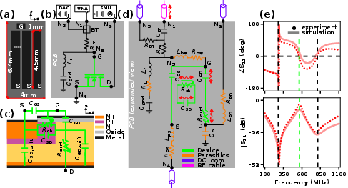
Figure 1: Measurement and modeling schematics for the SiC vertical MOSFET, including RF/DC integration and the dominant parasitic pathways.
The circuit model is comprehensive, incorporating device-internal resistances (notably channel and drift region), capacitive couplings between all terminals, bond-wire and PCB parasitics, and allows numerical simulation of the reflection coefficient S11. This is essential for separating signal contributions associated with intrinsic device physics versus those from circuit-level parasitics.
Room-Temperature Characterization
The MOSFET exhibits conventional behavior in DC transport with a threshold voltage VthRT≈1.5 V and RDS,onRT in the sub-ohm regime, matching manufacturer specifications.
A robust, gate-dependent RF reflectometry signal is detected at f0≈566 MHz, even with input parasitic capacitances on the order of nanofarads, which typically would be expected to degrade reflectometry. The frequency-dependence of the gate response, the magnitude of ∣ΔS11∣, and its reproducibility are analyzed. Numerical simulations using the detailed circuit model show that reflectometry sensitivity at room temperature is dominated not by the gate-channel capacitance but by resistive changes, particularly in the drift region, which are strongly modulated by gate voltage in the sub-threshold regime.
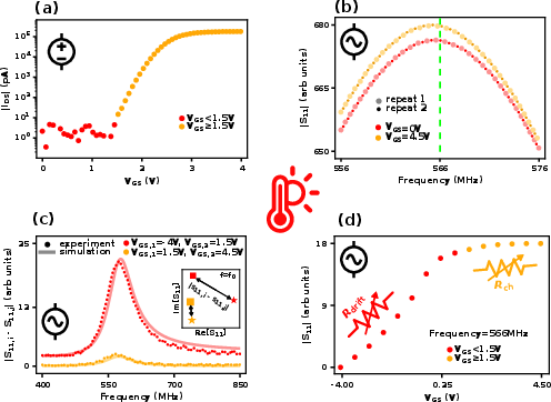
Figure 2: Room-temperature DC and RF characteristics, illustrating threshold behavior and strong gate-dependent S11 response primarily below the threshold.
The maximal sensitivity is observed for VGS<Vth, indicating that the in situ RF circuit senses depletion and resistance modulation in the drift region beneath the gate, rather than channel inversion. The quantitative agreement between measurement and model, and the failure of capacitance-based explanations for ∣ΔS11∣, underscores the fundamentally resistive nature of the dominant RF pathway in this geometry.
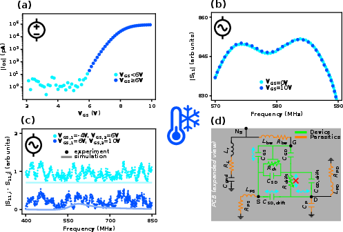
Figure 3: Cryogenic DC and RF characterization, showing preserved DC switching but vanishing S11 contrast as T→28 K.
Cryogenic Limitations and Physical Interpretation
At VthRT≈1.5 V0 K, the MOSFET still performs in DC transport, albeit with increased threshold (VthRT≈1.5 V1 V) and on-resistance (VthRT≈1.5 V2 kVthRT≈1.5 V3). However, the RF reflectometry response collapses: no significant change in VthRT≈1.5 V4 is detectable over the entire gate range and frequency window.
Simulations indicate that the loss of sensitivity is directly correlated with a sharp increase in drift region resistance due to carrier freeze-out below 50 K. When VthRT≈1.5 V5 exceeds the shunt impedance of dominant parasitic paths, the portion of the resonant RF current that samples gate-dependent device regions becomes negligibly small; circuit sensitivity to those resistances is lost. Instead, the RF current diverts entirely through high-capacitance, gate-independent pathways (e.g., VthRT≈1.5 V6, VthRT≈1.5 V7), rendering the reflectometry scheme insensitive to the active region of the device.
Engineering Solutions: Circuit Redesign
To overcome the fundamental loss of sensitivity at low temperature, a modified circuit topology is proposed. This redesign introduces additional capacitive and inductive elements at both the source and drain terminals to maximize the fraction of RF current traversing gate-dependent impedances (chiefly VthRT≈1.5 V8) while simultaneously suppressing leakage into external DC wiring.
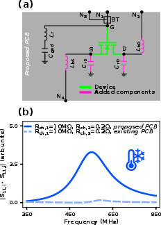
Figure 4: Modified PCB/circuit architecture and simulation, showing restored sensitivity to channel resistance with additional selective capacitive and inductive elements.
Theoretical modeling demonstrates that, for the modified circuit, sensitivity to VthRT≈1.5 V9 is significantly restored even when RDS,onRT0 is large. This approach confines oscillatory current within the effective channel-gating loop by leveraging added inductive chokes and capacitive bridges to ground, overcoming the current redistribution that otherwise occurs due to large drift-region resistance at cryogenic temperatures.
Implications for Scalable Quantum Hardware
The study clarifies that design of scalable cryogenic-CMOS quantum-classical interfaces must thoroughly account for the interplay between device internal physics (e.g., freeze-out of carriers, resistive and capacitive pathways modulated by gate bias and temperature) and full-system circuit topology (dominant RF current loops, PCB and interconnect parasitics). The observed suppression of reflectometry sensitivity at low temperature in large-area devices is a proxy for challenges likely to arise in dense, multiplexed quantum-classical integrated circuits, where unwanted parasitic shunt paths may similarly dominate.
The proposed circuit-level solution is generic in its design principles and could be adapted to improve RF readout in other contexts, such as large arrays of quantum-dot or single-electron devices, provided one identifies and re-routes dominant RF loops for maximal overlap with gate-dependent quantum impedances.
Conclusion
This work establishes, through detailed experiment and modeling, that in large-area SiC MOSFETs with substantial parasitic capacitance, RF reflectometry at room temperature remains viable and is governed by resistive variations in the drift region. However, a pronounced loss of RF signal at cryogenic temperature arises from the increase in drift-region resistance and consequent redistribution of RF current along parasitic, gate-independent pathways. Circuit-level reengineering—specifically, inclusion of capacitors and inductors to shape the RF current distribution—can restore reflectometry sensitivity to gate-dependent impedance changes, even under conditions of carrier freeze-out. The findings provide a blueprint for the architecture of scalable, high-sensitivity cryogenic-CMOS systems, and highlight the need for holistic device-circuit co-design in future quantum hardware.
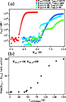
Figure 5: Maximum RDS,onRT1 contrast and gate-controlled DC characteristics as a function of temperature, illustrating the sharp degradation of RF sensitivity at cryogenic temperatures.

