- The paper presents a method using nanosecond-pulsed laser ablation to remove transport-blocking defects in surface-electrode ion traps.
- It details a progressive power ramping procedure that restored ion shuttling with a post-ablation error rate as low as 1.3×10⁻⁴ over 22,500 trials.
- The study confirms that the technique preserves adjacent electrode integrity and is compatible with cryogenic, multi-module quantum systems.
In Situ Ablation Removal of Transport-Blocking Defects in Surface-Electrode Ion Traps
Introduction
The integrity of ion transport pathways is fundamental to the operational reliability and performance of surface-electrode ion traps in quantum information processing architectures. The proliferation of complex shuttling procedures across multi-zone and modular designs places stringent demands on defect mitigation, as even single transport-blocking debris can inhibit downstream operations and cause lengthy experimental interruptions. This paper provides a formal characterization and demonstrable solution for the in situ removal of sizable transport-blocking defects using nanosecond-pulsed laser ablation, circumventing the necessity of vent–bake cycles and minimizing operational downtime.
Characterization of Defect and its Impact on Ion Transport
A transport-blocking defect was detected within a two-module quantum processor trap, specifically obstructing the shuttling path between the gate and adjacent module. High-resolution imaging and EMCCD-guided laser scanning established the defect dimensions to be approximately 65 μm in height and 40 μm in width—a scale sufficiently prohibitive to ion transport and thermometry measurements.
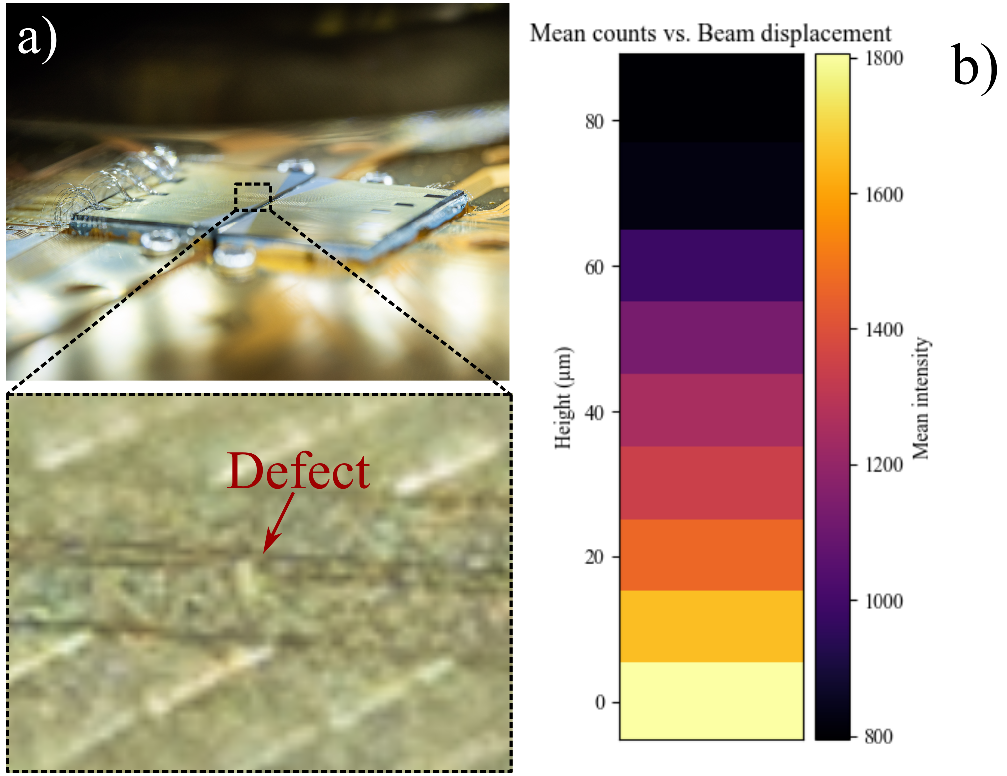
Figure 1: Side-view image and pixel scan of the defect, confirming its transport-blocking geometry with a height of 65 μm.
The practical implication is significant: high-fidelity shuttling is required for fast algorithmic execution, multiplexed operations, and modular integration. The presence of a defect at such a critical junction mandates robust remediation methods, particularly as conventional approaches (vent and rebake) are not tenable for cryogenic or multi-module systems due to extended downtime and added risk.
In Situ Nanosecond-Pulsed Ablation Methodology
The remediation protocol leveraged a Q-switched Nd:YAG laser at 532 nm, delivering 1.5 ns pulses with selectable fluence up to 2 mJ. Complementary continuous-wave (CW) 532 nm guide laser was employed for precise spatial targeting to the defect. The combined beams, manipulated via a micrometer translation stage, were focused to the defect’s location using a 150 mm lens. Beam expansion techniques centered on Gaussian conditioning and selective exposure were integrated to substantially reduce risk to neighboring electrodes.
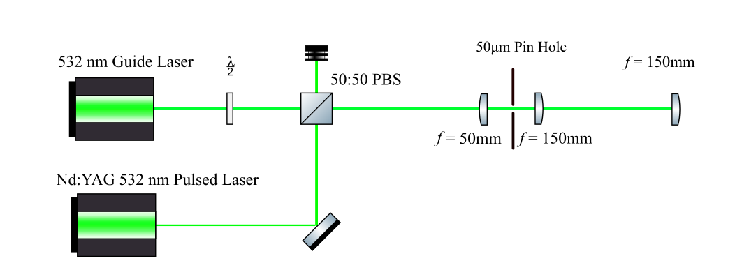
Figure 2: Beam path schematic illustrating overlapping guide/ablation lasers and the telescope ensuring spatial beam quality and alignment.
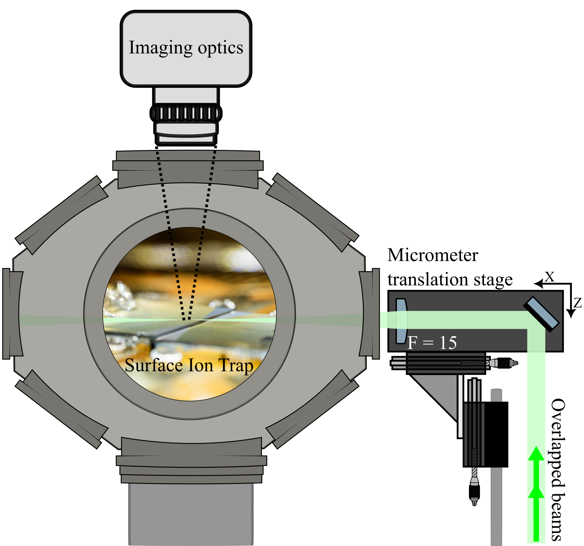
Figure 3: UHV system schematic showing the layout of the surface ion trap, imaging, and dual-laser ablation setup with precise XZ alignment.
Empirical ablation thresholds for constituent trap materials (Au, Al, steel) guided fluence calibration. Gold electrodes presented the highest risk, but the peak fluence incident on these components (1.9×10⁻³ J/cm²) remained well below typical ablation thresholds (1–4 J/cm²), confirming selective ablation at the defect site and preserving adjacent electrode integrity.
The method involved progressive ablation pulse power ramping from 10% to 80%, corresponding to target fluence increments from $0.56$ J/cm² to $6.8$ J/cm². At $5.6$ J/cm², total removal of the defect was achieved, evidenced by disappearance of guide laser scattering and confirmation via high-magnification imaging.
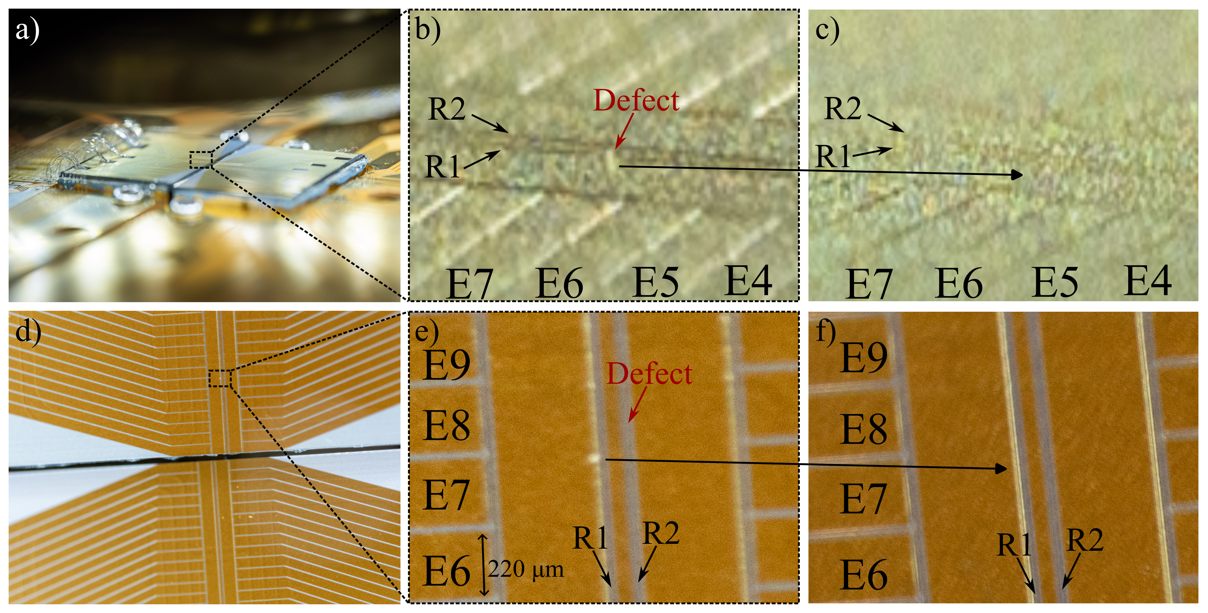
Figure 4: Multi-perspective images of the ion trap pre- and post-defect removal, including magnified views of the affected region and surface restoration.
The immediate outcome post-ablation was full restoration of shuttling across the previously blocked channel, with empirical round-trip shuttling error rate ≤1.3×10⁻⁴ over 22,500 trials. Prior to ablation, ion loss was absolute (>300 trials), demonstrating the efficacy of the laser-based approach for operational recovery.
Residual Perturbations and Micromotion Compensation
Photon-correlation measurements characterized residual RF pseudopotential distortions after defect removal. Compensation voltages required along the shuttling path demonstrated a localized perturbation at the defect site, consistent with the formation of a shallow crater. The maximum induced ion displacement (40 μ0m) aligned with typical shuttling operation tolerances, and compensation voltages remained within laboratory norms.
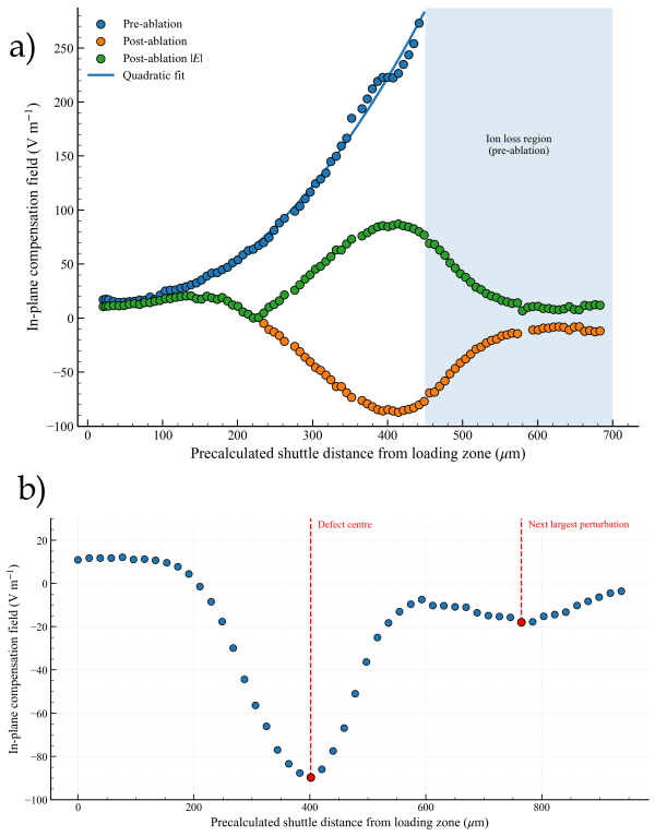
Figure 5: Spatially resolved micromotion compensation voltages highlighting pre- and post-ablation perturbations and restoration.
No observable damage to adjacent electrodes or degradation in trapping performance was found, and device functionality was uncompromised. The absence of disconnected or shorted DCs post-ablation further substantiates the selectivity and safety of the procedure.
Implications and Prospects for Quantum Device Maintenance
The in situ laser ablation protocol offers a viable low-overhead solution for defect remediation in surface-electrode ion traps, particularly for architectures where vent–bake cycles are infeasible. It enables rapid resumption of quantum operations while avoiding risks of alignment loss or prolonged downtime inherent in conventional cleaning strategies.
Practically, the approach is directly compatible with cryogenic operation and multi-module systems, serving as a tool for maintaining transport reliability and operational stability as ion trap platforms scale. The methodology’s selective nature implies utility not only for ion traps but also across other vacuum-housed microfabricated quantum devices, such as superconducting circuits and hybrid optomechanical systems, where localized defect removal is required.
Theoretically, this advancement strengthens the resilience of modular and shuttling-based architectures against particulate contamination, supporting greater system uptime and reliability. Extending ablation protocols to finer control and automation could enable real-time defect management, further cementing the noninvasive maintenance paradigm for quantum hardware.
Conclusion
This study presents a formal demonstration of in situ nanosecond-pulsed laser ablation for the removal of transport-blocking defects in surface-electrode ion traps. The technique achieves high success rates in restoring ion transport with minimal residual micromotion and no collateral electrode damage. Its compatibility with cryogenic and modular systems positions laser ablation as a practical, scalable tool for sustaining the operational reliability of advanced trapped-ion quantum processors and other vacuum-based quantum devices. Future developments may focus on automated defect detection and targeted ablation protocols for extended applications in quantum device maintenance.
(2605.06312)

