- The paper establishes a novel regime by integrating femtosecond pump–probe excitation with THz-STM to measure ultrafast band bending at individual atomic defects.
- It identifies three key mechanisms—terahertz field-induced rectification, sub-cycle photocurrent modulation, and terahertz-driven electron capture—through detailed differential conductance analysis.
- The work reveals spatially varying carrier decay times and defect-mediated band modulation, advancing nanoscale spectroscopy for optoelectronic materials.
Femtosecond Tunneling Spectroscopy of Ultrafast Band Bending Dynamics at the Atomic Limit
Introduction
This work establishes a robust regime for ultrafast tunneling spectroscopy at atomic spatial resolution by combining lightwave-driven terahertz scanning tunneling microscopy (THz-STM) with femtosecond optical pump–probe excitation. Direct measurement of ultrafast carrier dynamics and associated band bending phenomena is achieved at individual atomic defects on the GaAs(110) surface. Leveraging the sensitivity of STM to local electrostatic potentials and band alignment, and employing terahertz time-domain spectroscopy (THz-TDS) in the tip near-field, the authors disentangle sub-cycle dynamics directly induced by the terahertz driving field from the photoinduced intrinsic electronic response of the material.
Experimental Framework and Measurement Concept
The experimental platform integrates atomic-scale THz-STM and THz-TDS with femtosecond near-infrared optical pulses (810 nm, 50 fs) for pump–probe spectroscopy. The terahertz pulses, split into strong-field and weak-field components, provide sub-cycle temporal resolution while preserving picometer-scale spatial precision. Cross-correlation sampling of the terahertz waveform in situ at the tip apex enables robust characterization of the probe field irrespective of photocarrier injection, critical for accurate extraction of time-dependent differential conductance.
The silicon-doped GaAs(110) sample, with a screened plasma frequency of 18 THz, exhibits spatially nonuniform band-bending due to the distribution of defects and dopants (primarily Ga vacancies and Si substitutionals). STM and THz-STM images reveal spatial features consistent with defect-induced band bending, with positive terahertz-induced currents localized to defect centers.
(Figure 1)
Figure 1: Multidimensional pump–probe terahertz nanospectroscopy visualizes carrier-induced band bending and THz-field-driven tunnel currents at individual atomic sites of GaAs(110).
Mechanisms of Ultrafast Tunnel Current Generation
Three principal mechanisms are resolved:
- Terahertz Field-Induced Rectification: At sufficiently high terahertz bias across the tunnel junction, transient tunnel current surges are observed that outstrip the static STM current setpoint. The opening of new tunneling channels, including tip-to-valence/conduction band and resonant tunneling into surface states like C4 above the conduction band, dominate in the presence of strong band bending near defects.
- Sub-cycle Photocurrent Modulation: Near-infrared photoexcitation drives substantial transient photocurrents via carrier redistribution, giving rise to band flattening and modulation of surface state occupation. Weak terahertz fields modulate these photocurrents on sub-picosecond timescales, tracing the field polarity and temporal overlap between pump and probe.
- Terahertz-Driven Electron Capture: Broadband terahertz pulses seed electrons from bulk dopant states (e.g., Si donors) into the conduction band, with carrier lifetimes exceeding those of photoexcited electron–hole pairs. The bias dependence of electron capture, and its persistence at negative pump–probe delay times, is attributable to the shallow dopant potential and long-lived, non-equilibrium carrier population.
(Figure 2)
Figure 2: Simulated band alignment diagrams reveal key mechanisms: terahertz-field-induced rectification, sub-cycle photocurrent modulation, and electron capture—all modulated by tip and defect proximity.
Ultrafast Manipulation and Topographic Mapping of Band Bending
Quantitative Poisson solver simulations delineate the spatially resolved interplay of tip-induced and defect-induced band bending. The C4 surface state serves as a local spectroscopic marker, exhibiting maximum sub-cycle modulation at specific tip–defect lateral distances where the defect- and tip-induced potentials align C4 near the tip Fermi level.
STM and THz-STM constant-current images typify long-range topographic depressions surrounding charged defects, corresponding to regions where C4 is elevated above εF,tip. Variations in STM bias shift these regions, directly mapping the dynamic evolution of defect-mediated band bending in response to external fields.
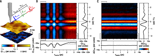
Figure 3: Ultrafast and bias-dependent tip-induced band topography visualized across single and multi-defect complexes, with rings of maximum photocurrent modulation and voltage-dependent spatial constraints.
Sub-cycle Differential Conductance and Atomic-Scale Dynamics
Point spectroscopy at distinct tip locations across the defect landscape reveals localized differences in two-dimensional maps of rectified charge QTHz(ETHz,pk,τpump). Decomposition into the three processes—rectification, photocurrent modulation, and electron capture—is enabled by fitting to a composite model (error functions for threshold processes, Gaussian for photocurrent modulation) convolved with the measured terahertz near-field waveform.
The extracted population decay times for photocurrents and electron capture exhibit strong spatial dependence, with photocurrent decay ranging from 580 fs at defects to 910 fs in pristine regions. These lifetimes are critical for resolving the temporal offset between true pump–probe overlap and signal maximum, and for mapping the actual carrier redistribution dynamics at the atomic limit.
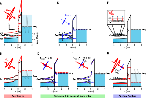
Figure 4: High-resolution differential conductance spectroscopy assesses local carrier lifetimes, field thresholds, and process decomposition at atomic defects and pristine surfaces.
Implications and Outlook
This work establishes a rigorous spectroscopic methodology for the direct visualization and quantification of ultrafast carrier dynamics, band realignment, and defect-mediated charge redistribution at atomic resolution. The field-insensitivity of the terahertz probe waveform to photoexcitation allows robust extraction of the intrinsic time-dependent differential conductance without convolution artifacts.
Future developments may extend this approach to more complex material systems—heterostructures, 2D materials, quantum platforms—where band alignment, defect states, and local dielectric function are intricately coupled. Simultaneous measurement of ultrafast dynamics in the local density of states and dielectric function at the atomic scale promises unprecedented insight into carrier transport, defect engineering, and optoelectronic device design. Challenges remain in fully decoupling rectified charge signatures from dielectric function evolution when both respond dynamically to pump-driven excitation, requiring more sophisticated modeling and inversion techniques.
Conclusion
The combination of femtosecond optical pump–probe excitation, atomic-scale THz-STM, and in situ THz-TDS enables the direct tracking of ultrafast band bending dynamics, carrier redistribution, and transient electronic structure at individual defect sites. By establishing a clear relationship between time-resolved differential conductance and local carrier filling, this work provides a powerful framework for interrogating and engineering nonequilibrium processes in tunable optoelectronic materials at their fundamental limits.

