- The paper introduces a reconfigurable three-nTron superconducting logic gate that processes SNSPD outputs to perform AND, OR, and XOR logic operations.
- The authors validate the device at 4.2 K using time-domain measurements, achieving bit-error rates below 10⁻³ and bias margins up to ±24% for robust performance.
- Its integration with SNSPDs and compatibility with electro-optic modulators showcases its potential for scalable, low-power quantum photonic processors.
Reconfigurable Superconducting Logic for On-Chip Photon Coincidence Detection
Introduction and Context
The presented work addresses one of the principal bottlenecks in scaling photonic quantum-information platforms: low-latency, on-chip processing of single-photon detection events. The proliferation of large arrays of superconducting nanowire single-photon detectors (SNSPDs) is central to photonic quantum computation, communication, and sensing. However, classical feedforward control, particularly the conditional operation of modulators and switches based on multi-detector outcomes such as Bell-state measurements, is fundamentally limited by the latency and wiring complexity inherent to room-temperature electronics. Conventional solutions, such as cryo-CMOS and RSFQ logic, introduce overhead in fabrication and power dissipation, and often require complex impedance matching to interface effectively with SNSPD outputs.
This work reports the design, fabrication, and experimental characterization of a bias-reconfigurable superconducting logic gate based on three nanocryotrons (nTrons), leveraging the same thin-film NbN platform as the SNSPDs. This gate performs native on-chip processing of SNSPD output pulses and provides AND (coincidence), XOR (odd-parity), and OR logic in a single programmable device, with bias-programmable configuration and self-resetting operation.
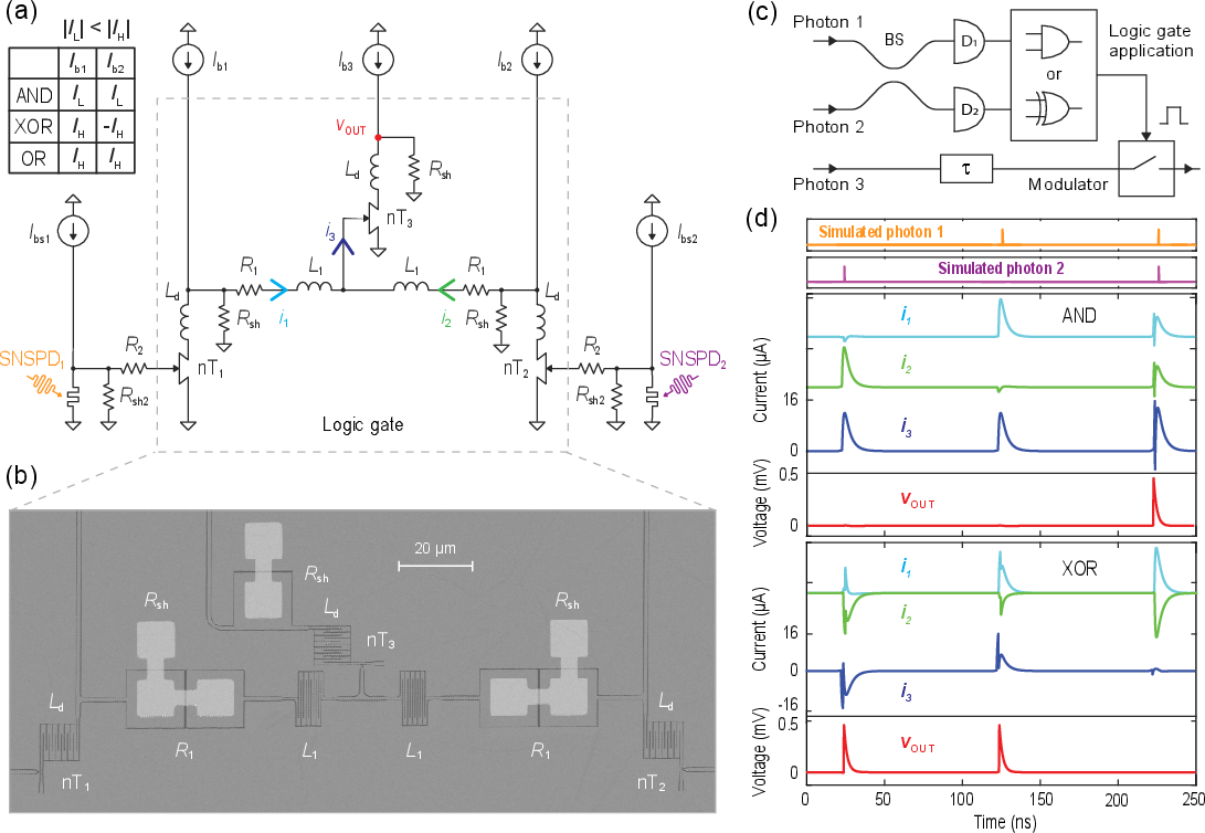
Figure 1: Schematic, micrograph, and simulated operation of the three-nTron reconfigurable logic gate coupled to SNSPDs.
Device Architecture and Operating Principle
The gate consists of two side nTrons (nT1 and nT2), each driven by one SNSPD, and a central nTron (nT3) that constitutes the output stage. Input pulses from the SNSPDs induce switching in the side nTrons, which, through current redirection—modulated by the device bias—collectively determine the drive for the central nTron. The bias currents Ib1 and Ib2 set the functional mode: AND (realizing coincidence logic), OR, or XOR (photon bunching selectivity), by controlling the constructive or destructive addition of output currents at nT3.
Self-resetting operation is achieved using shunt resistors at each nTron, which eliminate the need for external reset signals and for additional energy-dissipating circuitry. This design, realized using standard nanopatterned NbN and Ti/Au thin-film resistors, directly interfaces electronic and photonic layers with minimal fabrication overhead or impedance-matching requirements.
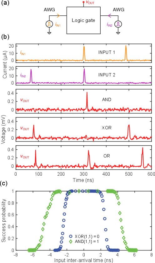
Figure 2: Experimental verification of gate reconfigurability and timing dependence with waveform-generated inputs.
Experimental Characterization
Logic Fidelity and Timing Window
Extensive characterization at 4.2 K using arbitrary waveform generator (AWG) pulses demonstrates high-fidelity operation with bit-error rates (BER) below 10−3 for all logic configurations in optimal bias windows. Time-domain measurements confirm the expected logic outputs and the programmable transition between AND, XOR, and OR functions. The timing window for correct operation, critical for coincidence logic, is set by the device L/R time constants and pulse shape; the AND mode provides a tolerance of ∼7.7 ns (90% probability), and the XOR mode supports a narrower 4.1 ns window due to its sensitivity to pulse overlap and cancellation.
Bias Margins and Robustness
Comprehensive BER mapping as a function of Ib1 and Ib2 reveals wide bias windows, notably 2024% for OR, 2115% for AND, and 2214% for XOR operation, underlining the device’s tolerance to parameter drift and device non-uniformity.
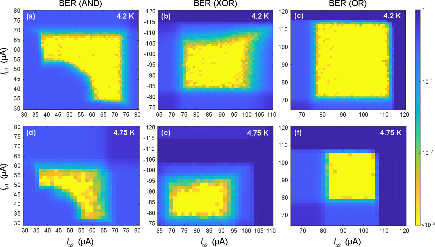
Figure 3: Bias space mapping of bit-error-rate (BER) for each logic configuration at two temperatures.
Temperature dependence studies show functional operation persists as device critical currents reduce at elevated temperatures (to 4.75 K), with a contraction of the bias windows but preserved configurability. Operation up to 25 MHz is verified, with the understanding that the speed limit is mainly imposed by the inductive reset time and ultimately the hotspot relaxation time of the nanowires, which is substrate-dependent.
Power Dissipation
Simulations of the device in experimental conditions report per-operation energy dissipation of 7.4–7.6 fJ for 5 ns pulses, with average instantaneous power around 1 μW, matching the best reported for nTron logics but higher than for RSFQ/JJ logic, commensurate with the higher operating impedance and output drive capabilities.
SNSPD Integration and Native Photon Event Processing
Integration with on-chip SNSPDs is demonstrated using two co-fabricated detectors coupled to the logic gate via direct wire bonds and surface-mount resistors. Experimental operation under optical excitation with a pulsed 1550 nm laser shows the correct AND and XOR logic on detection events, with BERs of 23 (AND) and 24 (XOR) using 10,000 events, despite sub-optimal coupling and the presence of afterpulsing in the detectors. Timing windows up to 19 ns (AND) and 26 ns (XOR) are allowed for output pulse acceptance.
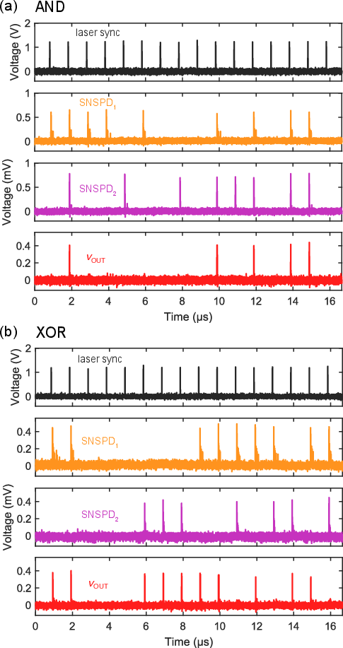
Figure 4: Experimental traces showing correct AND and XOR processing of SNSPD-generated pulses with the reconfigurable logic gate.
The dominant error sources are identified as afterpulses and uncertainties arising from the electrical coupling and impedance mismatch in the test setup. The authors highlight that fully integrated, wire-bond-free integration or use of optimized coupling, as shown in prior work, would further suppress BER and timing jitter.
Compatibility with Optical Modulation Stages
A critical requirement for photonic feedforward is sufficient output drive to control fast electro-optic modulators operating at volt-level amplitude. The authors demonstrate that a wide-channel nTron can drive a 1 pF capacitive load (representative of an electro-optic modulator) to 1.15 V with 5 ns, 68 μA input pulses at 100 kHz, thus supporting the feasibility of this approach for directly actuating subsequent optical elements in an integrated photonic quantum circuit.
Implications and Future Directions
This study establishes a platform for fully reconfigurable, cryogenic logic compatible with high-performance photon-number detection, eliminating the need for room-temperature electronics and reducing system-scale wiring. The device's bias-reconfigurability enables a universal set of logic operations (AND, OR, XOR, and via external pulsing, NAND and NOT), facilitating flexible implementation of quantum measurement protocols, classical feedforward, or error-correction logic without redesign or re-patterning.
Practically, this level of integration paves the way for large-scale, fast, and low-power on-chip quantum photonic processors, with straightforward extension to multi-gate logic, enhanced error correction, and eventually, tightly-coupled digital-analog superconducting computation in extreme environments. The design is inherently adaptable to a variety of superconducting materials compatible with current photonic integration pipelines, and is scalable within the lithographic constraints of existing fabrication.
Further optimizations are foreseen in device speed, coupling efficiency, and noise suppression, through advanced materials (e.g., epitaxial NbN), improved architecture for rapid thermal recovery, and monolithic electronic-photonic integration. Fully co-integrated logic and SNSPD modules interfacing with high-speed modulators or complex photonic circuits will support real-time quantum information processing and large-scale quantum networking.
Conclusion
The reconfigurable three-nTron gate advances the state-of-the-art in superconducting logic for quantum photonic systems. It demonstrates millivolt-level, bias-programmable AND, OR, and XOR logic on native SNSPD outputs at 4.2–4.75 K with low error rates, wide operating margins, and power levels suitable for scaling. With output drive compatible with electro-optic modulation, this architecture is a compelling building block for future, fully integrated quantum feedforward, multiplexed detection, and scalable on-chip photonic control systems (2604.22101).