- The paper introduces a novel nanophotonic platform that enhances photon-nucleus interactions in 229Th nuclear clocks using high-Q fluoride resonators.
- The paper combines experimental 229Th implantation in MgF2 whispering-gallery-mode resonators and semiclassical modeling to quantify excitation rates and photon flux dynamics.
- The paper demonstrates that milliwatt-level pump powers and optimized device architectures can achieve detection thresholds for practical chip-scale frequency standards.
Introduction
This paper develops a nanophotonic platform for realizing all-solid-state frequency standards based on the 229Th nuclear isomer, targeting chip-scale nuclear clocks by embedding thorium nuclei within high-Q fluoride photonic resonators. Leveraging advances in materials integration, resonator fabrication, and optonuclear coupling, it addresses the optical manipulation and interrogation of the low-energy 8.4 eV nuclear transition, outlining a quantitative framework for enhanced excitation rates, resonator-assisted photon emission, and scalable device architectures. Experimental proof is offered via successful implantation of 229Th into MgF2 whispering-gallery-mode (WGM) resonators and the characterization of device performance. The paper systematically analyzes photon-nucleus interaction dynamics, fabrication constraints, and technology roadmaps for on-chip laser and detection integration.
Physics of Nucleus-Photon Interaction in Nanophotonic Resonators
The main technical advance is the integration of 229Th nuclei into high-Q WGM fluoride resonators transparent in the VUV, achieving substantial enhancement in nuclear excitation rates due to field confinement and resonance. Nanophotonic cavities amplify local photon densities, thus increasing both single-photon and two-photon nuclear excitation cross sections. The dominant M1 channel yields a nuclear transition half-life of 1740 s in vacuum; direct one-photon absorption cross sections are inversely proportional to laser linewidth, while two-photon cross sections require high pump intensities but can be enhanced by the optonuclear quadrupolar effect (ONQ) in solid-state hosts.
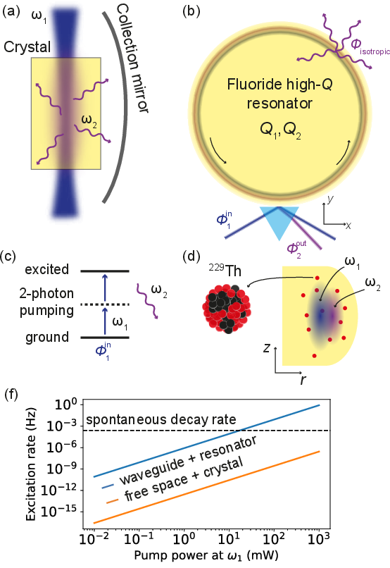
Figure 1: Depiction of conventional and cavity-enhanced pumping schemes for thorium-doped crystals utilizing high-Q WGM resonators, illustrating mode overlap and excitation efficiency.
Theoretical modeling employs semiclassical rate equations for nuclear population inversion and cavity photon numbers, incorporating Purcell-enhanced emission, spatial mode overlap, and decoherence effects from the host matrix. Simulations indicate milliwatt-level pump powers, high-Q (∼106), and thorium densities (2290) achieve detectable photon fluxes for both one-photon and ONQ-assisted two-photon excitation mechanisms.
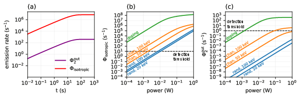
Figure 2: Modeled photon flux dynamics for two-photon pumping, including cavity output and isotropic emission rates as functions of pump power and implantation strategy.
Notably, ONQ-mediated two-photon excitation is projected to outperform direct nuclear two-photon absorption by many orders of magnitude. Quantitative estimates show cavity output photon fluxes readily surpass detection thresholds in both bulk-doped and high-activity surface-implanted configurations, validating practical device concepts.
Fabrication and Characterization of 2291Th-Implanted WGM Resonators
Device realization utilizes two main strategies: homogeneous bulk doping and post-fabrication ion implantation. The latter enables precise localization of thorium nuclei within high-intensity mode regions near resonator surfaces, maximizing photon-nucleus interaction and minimizing radioluminescence background from non-overlapping nuclei. Initial experiments on MgF2292 WGM resonators demonstrate successful 2293Th implantation, depth profile optimization, and minimal degradation of optical 2294-factors via low-energy, channeled implantation and annealing.
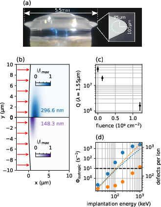
Figure 3: Photograph and simulation of 2295Th-implanted MgF2296 WGM resonator, showing mode intensity profiles, implantation direction, measured 2297-factors, and projected nuclear fluorescence rates.
Simulated implantation profiles and mode field distributions predict that channeled implantation can achieve greater overlap with electromagnetic field regions at lower ion energies and defects compared to random incidence. Experimentally, defect densities created during implantation are quantified and strategies for further reduction are discussed, including high-temperature processing and post-annealing. Preliminary results indicate that photon emission rates from implanted nuclei in optimized resonators can meet or exceed detection thresholds under realistic pumping regimes.
Integrated Technology Roadmap: Laser Excitation and VUV Photon Detection
A pragmatic device architecture requires high-performance, tunable, narrow-linewidth laser sources at the excitation wavelength (either 148.4 nm for direct one-photon or 296.8 nm for two-photon ONQ excitation). Direct commercial lasers at 148.4 nm remain experimentally scarce; however, integrated photonic platforms (e.g., PPLN/PPLT, AlN, AlGaN, h-BN) enable efficient frequency doubling schemes, extending coverage down to the critical UV regime and providing watt-level output. The roadmap includes a chip-scale system featuring integrated diode lasers, microring resonator stabilization, sequential frequency doubling, and butt-coupling to WGM resonators—permitting compact, manufacturable frequency references.
Vacuum-ultraviolet (VUV) photon detection in integrated devices is approached via semiconductor detectors (AlN, AlGaN, diamond, h-BN), microchannel plate photomultiplier tubes (2298PMTs), and scintillator materials (ZnO, YAG:Ce, perovskites). Waveguide-coupled or thin-film bonded arrays allow single-photon sensitivity and scalable readout. The roadmap identifies direct coupling schemes for VUV emission out of fluoride resonators into detector elements, optimizing both efficiency and spatial resolution.
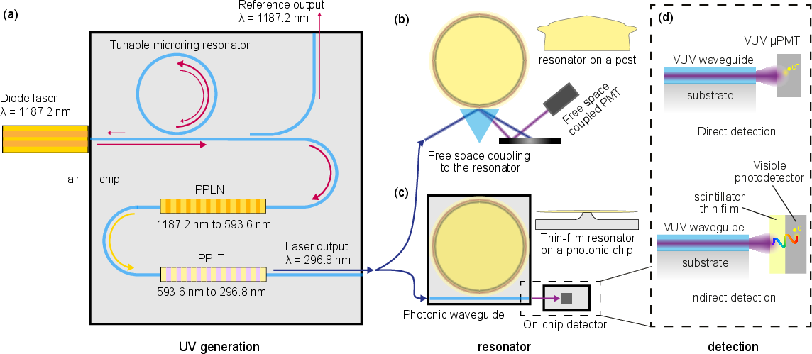
Figure 4: Schematic of miniaturization and integration pathways including on-chip tunable laser, free-space excitation, fully-integrated fluoride photonic platforms, and methods for on-chip VUV photon detection.
The paper delivers strong claims in demonstrating that milliwatt-level pump powers, realistic 2299-factors, and thorium densities yield photon fluxes in the VUV detectable via current chip-compatible detectors, confirming the feasibility of solid-state nuclear frequency references. The solid-state approach enables orders-of-magnitude scaling in nuclear emitter density, compact device footprint, and robust deployment—contrasting with gas-phase atomic clock architectures. Theoretical modeling and device engineering address critical systematic uncertainties such as radioluminescence background, implantation-induced lattice defects, and host crystal temperature sensitivity.
Device stability benchmarks projected in the literature suggest fractional uncertainties approaching Q0, while referenced experiments demonstrate linewidths, reproducibility, and environmental insensitivity suitable for quantum metrology and navigation use cases. The integration roadmap synergizes recent advances in photonic frequency combs, chip-scale clocks, and scalable nonlinear optics.
Looking forward, engineering periodic spatial distributions or phase-matching strategies for coherent superradiant buildup may further enhance clock stability and output power. Further optimization in wafer-scale fluoride fabrication, on-chip frequency conversion, and detector integration is anticipated to yield mass-manufacturable, field-deployable solid-state nuclear clocks. Such systems additionally hold promise for fundamental tests of temporal variation in physical constants and quantum control of nuclear transitions.
Conclusion
This work establishes a comprehensive framework and practical demonstration for nanophotonic platforms in solid-state Q1Th nuclear clocks, encompassing photon-nucleus interaction modeling, resonator fabrication, thorium implantation, excitation schemes, and detection strategies. The combined theoretical and experimental approach provides a realistic path toward chip-scale nuclear frequency standards that leverage high-density solid-state nuclear ensembles, nanophotonic cavity enhancement, and advancing photonic integration. The results support further exploration of coherent collective effects, optimization of material architectures, and on-chip photonic clock integration for applications in precision timing, navigation, and fundamental physics.