- The paper presents a new κ-engineered taper that significantly reduces footprint and improves inter-layer transition reliability.
- It demonstrates wafer-scale uniformity through innovative E-CMP planarization and stress release trenches, achieving low propagation loss (<0.08 dB/cm).
- The study validates the approach with statistical analysis over 21 dies and 4000 resonances, paving the way for high-density multi-layer PIC systems.
Reliable Wafer-Scale 3D Photonic Integrated Circuits and Cavities
Introduction
This work addresses the critical limitations in wafer-scale engineering of three-dimensional photonic integrated circuits (3D PICs), where scaling demands collide with device uniformity, inter-layer transition efficiency, and footprint constraints. The authors present a sequence of process innovations and a new taper design based on engineered coupling (κ-engineering), enabling reproducible, low-loss, and scalable 3D photonic architectures in silicon nitride (SiN). The methodological contributions are validated through rigorous statistical analysis across a 4-inch wafer, establishing pathways for high-density, highly functional photonic systems suitable for advanced communications, sensors, and nonlinear applications.
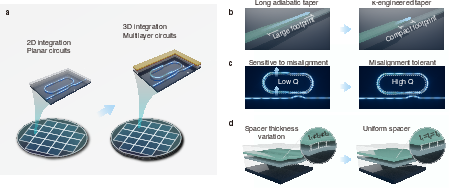
Figure 1: Key challenges in wafer-scale 3D PICs and solutions involving κ-engineered tapers for footprint-efficiency trade-off, and E-CMP for spacer uniformity.
Wafer-scale fabrication with SiN faces inherent challenges from film stress, particularly arising from CVD and high-temperature annealing required for optical performance. The resultant wafer bow induces critical overlay misalignments and vertical deviations in the inter-layer spacer, compromising yield and introducing non-uniformity in device performance. The solution integrates several key process steps: plasma-enhanced chemical vapor deposition (PECVD) affords low stress and repeatable SiN films, while a combination of stress release trenches (SRT) and etch-back assisted chemical mechanical polishing (E-CMP) provides spatial control of both lateral and vertical uniformity.
The E-CMP method utilizes nanoimprint lithography (NIL) resist for high step coverage, followed by targeted plasma etching and brief CMP cycles to produce highly uniform spacer layers. Quantitatively, the wafer-scale coefficient of variation (CV) for the bottom-to-bottom (B-B) distance (defining the inter-layer separation) is 2.06% with a kurtosis (β2) of $2.01$, evidencing tightly controlled spacer thickness over 4-inch wafers.
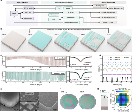
Figure 2: Process flow and outcomes for stress mitigation in 3D SiN PICs, including step coverage, planarization, and measurement of intra- and inter-layer uniformity.
Intrinsic waveguide losses on both SiN layers are simultaneously minimized, with typical propagation loss at $0.077$ dB/cm (L1) and $0.068$ dB/cm (L2), as characterized by high-Q ring resonators.
A central innovation is the κ-engineered taper, devised to resolve the longstanding trade-off between transition efficiency and taper length inherent to conventional linear adiabatic couplers. The standard linear taper (L-taper) localizes the phase-matching condition, demanding excessive lengths for high efficiency and proving highly susceptible to lateral and vertical misalignment. Instead, the κ-taper employs Hermite interpolation to flatten the coupling coefficient's spatial profile, thereby spatially broadening the efficient power transfer region and allowing significant footprint reduction.
Systematic fabrication and characterization show that, across taper lengths (κ0–κ1 κ2m) and lateral offsets (κ3–κ4 nm), the κ5-taper consistently achieves lower, less variant loss than the L-taper. For example, a κ6 κ7m κ8-taper outperforms an κ9 2.06%0m L-taper, and critical misalignment cases that render L-taper loss unmeasurable (e.g., 2.06%1 nm offset, 2.06%2 2.06%3m length) yield 2.06%4 dB/coupler in the 2.06%5-taper. The mean value of the reliability metric 2.06%6 across the experimental matrix shows a 2.06%7 improvement for the 2.06%8-taper over the L-taper.
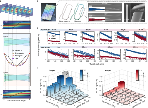
Figure 3: Design, SEM images, and systematic loss/robustness analysis of 2.06%9-taper versus L-taper, demonstrating footprint and reliability improvements.
Comprehensive wafer-scale characterization over β20 dies quantifies propagation and transition losses, measured from over β21 resonance dips per configuration. The β22-taper provides a statistical modal value for transition loss of β23 mdB/coupler (CV β24, β25 β26), outperforming the L-taper (β27 mdB/coupler, CV β28, β29 $2.01$0) not only in central tendency but in distribution narrowness, highlighting yield and robustness at scale.
At the device level, this enables the creation of 3D hybrid cavities that span multiple layers while maintaining intrinsic loss governed by single-layer waveguide loss, verified by high-Q performance across S, C, and L telecom bands. Notably, the transition loss approaches the intra-layer level, ensuring that inter-layer transfers do not become the bottleneck for advanced circuit architectures.
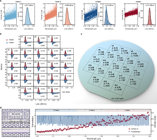
Figure 4: Wafer-scale statistics for loss in resonators and inter-layer transitions, and demonstration of high-Q hybrid 3D cavity exploiting the $2.01$1-taper.
Implications and Outlook
This paper’s approach simultaneously advances process control, design methodology, and device reliability in scalable 3D PICs. The integration of E-CMP planarization, SRT-based stress management, and $2.01$2-engineered tapers produces low-loss, highly uniform, and misalignment-tolerant architectures. These developments push PICs closer to the density, yield, and multifunctionality required for ultra-fast interconnects, scalable nonlinear platforms, and complex photonic computation. The compatibility with multilayer, heterogeneously integrated systems further enables the combination of active and passive materials without significant transition penalty.
Key open directions include extending $2.01$3-engineering to more than two layers, exploring multi-material vertical integrations (e.g., SiN/AlN, SiN/LiNbO$2.01$4), and leveraging the robust platform for quantum photonic, neuromorphic, and sensor network applications. Theory-guided tapering strategies may be further refined via inverse design or machine learning optimization as PIC complexity escalates.
Conclusion
The paper establishes a comprehensive foundation for manufacturing high-density, reliable 3D PICs and quantum-grade hybrid cavities at the wafer scale. By innovating both at the process and device levels, notably through the $2.01$5-taper and advanced planarization, the work achieves strong uniformity, minimal inter-layer loss, and enhanced misalignment tolerance, enabling scalable and multifunctional photonic systems. These contributions substantively advance the viability of photonic integration for next-generation classical and quantum information processing.
Reference:
"Building reliable 3D photonic integrated circuits and cavities at the wafer scale" (2604.12889)

