- The paper introduces a deterministic, polymer-free technique using muscovite mica, eliminating contamination from conventional polymer transfers.
- The method achieves atomic-scale cleanliness and precise twist-angle control, enabling ballistic transport and ultra-high mobility in vdW heterostructure devices.
- Experimental results show reduced interface roughness (<100 pm) and robust performance across various 2D materials including graphene and TMDs.
Polymer-Free Assembly of Van der Waals Heterostructures Using Muscovite Mica
Introduction and Motivation
The fabrication of van der Waals (vdW) heterostructures, composed of stacked two-dimensional (2D) crystals with atomically sharp interfaces, underpins advances in quantum materials research and device engineering. Conventional assembly methodologies predominantly utilize polymer-based transfer media (e.g., PMMA, PDMS, PC, PPC). Despite their widespread adoption, these approaches consistently introduce contamination, impose strain, and provide only coarse control over adhesion, thereby limiting device performance—particularly for high-mobility transport and precision-twisted electronic heterostructures. Recent alternatives leveraging freestanding 2D material or SiNx/metal cantilevers mitigate residue but present challenges in practical implementation, clean large-area assembly, and reproducible angular registration.
This work, "Polymer-free van der Waals assembly of 2D material heterostructures using muscovite crystals" (2604.12264), introduces a deterministic, all-dry, polymer-free protocol for vdW assembly, systematically replacing conventional polymer supports with atomically flat, optically transparent muscovite mica membranes or cantilevers. The approach exploits mica's tunable adhesion, mechanical rigidity, and chemical inertness, enabling thermal control over the pick-up, stacking, and release of 2D flakes without contaminating the heterointerface. This method demonstrates compatibility with established fabrication workflows and addresses critical limitations associated with polymer-assisted assembly and residue-free device construction.
Fabrication Methodology and Mechanistic Principles
The mica transfer protocol is based on the fine-tuning of van der Waals adhesion hierarchies: adhesion between mica and a 2D material (such as graphene or hBN) exceeds that to SiO2 substrates but is weaker than the intra-vdW adhesion in heterostructures. Using commercially available AFM-grade muscovite crystals, large-area (>100μm), thin (∼150–650 nm) mica membranes are prepared by micromechanical exfoliation. These membranes serve as polymer substitutes in either PDMS-supported membranes or freestanding cantilevers (with geometric and structural details shown in Fig. 1a–h).
After exfoliating the desired 2D crystal on SiO2, the substrate is pre-heated (50–90°C) to optimize adhesion differentials. The mica membrane is brought into controlled contact, where the pick-up front line is manipulated either geometrically (z-axis) or thermally (±10°C). Sequential stacking is possible by repeated pick-up, utilizing a temperature-driven reduction of mica-2D adhesion to release the stack onto a designed bottom layer (typically hBN or graphite), achieving high deterministic precision and retention of the twist angle. The robustness and reproducibility of the assembly protocol are validated across multiple device geometries.
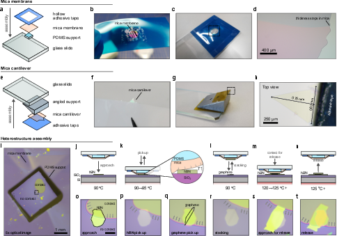
Figure 1: Protocol for mica-assisted heterostructure assembly—schematics and optical images of mica membrane and cantilever production, followed by stepwise device assembly.
Surface Cleanliness, Structural Integrity, and Heterointerface Characterization
Critical to high-performance vdW heterostructures is the minimization of interface roughness and contamination, typically compromised in polymer-based transfers. AFM characterization shows mica-assembled graphene/hBN stacks exhibit root-mean-square (RMS) interfacial roughness Rrms<100 pm over >100 μm2 areas, with no detectable polymer residues or extrinsic contaminants. Surface bubbles and contaminants are mechanically excluded from the device active regions by the controlled movement of the mica–substrate contact line at elevated release temperatures. These results are reproducible for both mica membrane and cantilever protocols, as demonstrated for various graphene/hBN, TLG/hBN, and multilayer electronically active stacks.
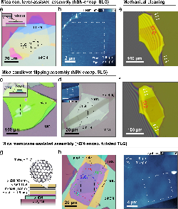
Figure 2: Optical microscopy and AFM images of hBN-encapsulated graphene assembled using mica stamps, illustrating atomic-scale surface flatness and defect-free regions.
Assembly and Characterization of Moiré Superlattices and Atomic Registry
The mica-assisted transfer enables precise control over rotational alignment for moiré superlattice formation, including marginally aligned hBN/hBN and SLG/hBN stacks, without compromising the twist angle—a feature frequently degraded by thermal drift in polymer-based assembly. High-throughput fabrication yields for moiré superlattices reach nearly 50%, primarily limited by layer count misassignments in thin hBN. KPFM and PFM reveal highly uniform ferroelectric domain patterns and moiré periodicity, which are preserved pre- and post-mica transfer—an essential requirement for optical and scanning probe studies of moiré physics. Comparative studies with PC-based methods illustrate that polymer residues screen or distort surface potentials and domain regularity, necessitating post-assembly cleaning, which the mica method intrinsically circumvents.
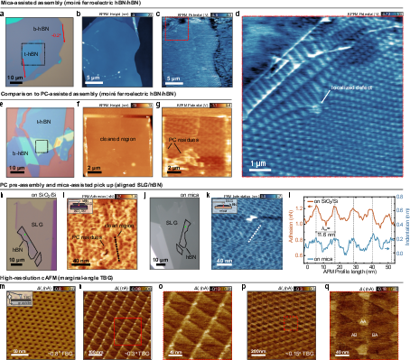
Figure 3: SPM-based characterization of moiré patterns and ferroelectric domains in hBN/hBN and graphene/hBN stacks assembled via mica, with direct comparison to polymer-assembled controls.
Devices manufactured via mica-assisted assembly achieve electronic performance on par with the leading reports for polymer-free processing, including sub-100 ppm disorder and high twist-angle uniformity. SLG/hBN Hall bars (20×14μm2) exhibit ballistic transport at 1.7 K, evidenced by negative non-local resistance and electron focusing effects, with mobility μ up to 20, limited by device geometry rather than material quality. In complex structures—such as 7-layer hBN/twisted TLG/hBN/graphite/hBN stacks—onset of Landau quantization at fields as low as 21 mT and the observation of 22 distinct Landau levels at 23 mT both signal exceptionally low charge impurity and high stacking precision. Critically, the method supports device fabrication with mica remaining in sub-stack geometries without loss of electronic quality or gate tunability.
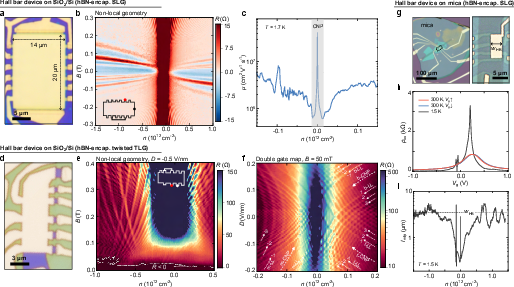
Figure 4: Low-temperature magnetotransport measurements in mica-assembled heterostructures, demonstrating ballistic transport, ultra-high mobility, and quantum Hall effect signatures.
Extension to Suspended Heterostructure Membranes and Non-Graphene 2D Systems
A salient feature of mica-assisted assembly is its ability to reliably fabricate suspended heterostructure membranes without post-process cleaning or annealing, overcoming limitations of low suspended device yield and interface contamination in liquid-assisted or CVD-transferred approaches. Suspended graphene/hBN membranes (24m) show mechanical properties (Young’s modulus 25 GPa, pre-tension 26) in agreement with prior measurements and reproducible frequency responses (27, 28 MHz), with pristine surface quality across the free-standing area. Suspended moiré membranes have been fabricated and characterized with PFM, validating uniformity over the entire surface.
This methodology further extends to air-sensitive and low-adhesion materials, including folded ferroelectric 3R-MoS29, monolayer MoS>100μ0, few-layer FePS>100μ1, and CrBr>100μ2. Properly optimized, mica transfer enables stacking, folding, and full encapsulation of these materials with atomic precision, minimal roughness, and no detectable residue.
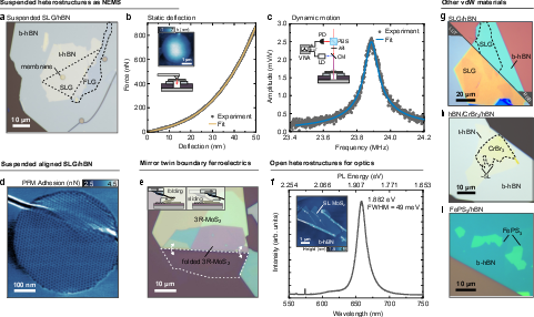
Figure 5: Functional devices based on mica-mediated assembly—suspended membranes, folded 3R-MoS>100μ3, photoluminescent monolayer TMD, and air-sensitive van der Waals assemblies.
Limitations, Practical Considerations, and Future Extensions
Despite unmatched surface cleanliness and deterministic control, scalability to wafer-scale or fully industry-compatible fabrication remains constrained by current manipulation protocols and release mechanisms, especially for non-hBN bottom layers. Challenges include optimal adhesion matching for diverse material classes and assembly under variable ambient/humidity, though the method demonstrates robust performance under standard laboratory conditions down to 50% relative humidity. All such obstacles are principally practical: muscovite mica is available in macroscopic crystals, which could, with development of automated or robotic assembly, enable industrial throughput and large-area integration. The extension to non-vdW systems (e.g., freestanding complex oxides, monolayer amorphous carbon) is posited, potentially expanding the technique’s utility to a broad array of atomically engineered heterostructures.
Conclusion
This work establishes a robust, versatile, and cost-effective polymer-free protocol based on muscovite mica for vdW heterostructure assembly. The method achieves atomic-scale cleanliness, strain minimization, and high determinism in twist-angle control. Devices assembled via this protocol exhibit ultra-high mobility, ballistic transport, well-defined quantum Hall signatures, and large-area uniform moiré order, without any need for post-fabrication cleaning or annealing. The practical implications are substantial: enabling reliable fabrication of clean, functional 2D heterostructure devices, unencumbered by polymer contamination, for both research and, with further development, possible industrial applications in advanced quantum and optoelectronic devices.
(2604.12264)