- The paper demonstrates that maskless EBIE leverages secondary electrons to dissociate ambient O₂/N₂ molecules, enabling precise etching of diamond with minimal damage.
- It reveals that varying SEM parameters such as electron energy, current density, gas flow, and dwell time establishes distinct molecule-limited and electron-limited regimes for controlled patterning.
- The study achieves etch depths up to 212 nm and lateral resolutions of 200 nm, showcasing its potential for advanced quantum, photonic, and nano-electronic device fabrication.
Maskless Electron Beam–Induced Etching of Diamond in Air: Mechanisms, Regimes, and Anisotropy
Introduction
Maskless electron beam–induced etching (EBIE) in air for diamond micro and nanostructuring represents a significant advance over traditional reactive ion etching (RIE) by enabling damage-free, direct-write patterning without lithographic masks or plasma exposure. The process leverages the unique interplay of electron–gas, electron–diamond, and gas–surface interactions within the scanning electron microscope (SEM) chamber. This work delivers a rigorous mechanistic analysis, resolves the role of secondary electrons (SEs), establishes operational regimes, and documents crystallographically selective etching under air.
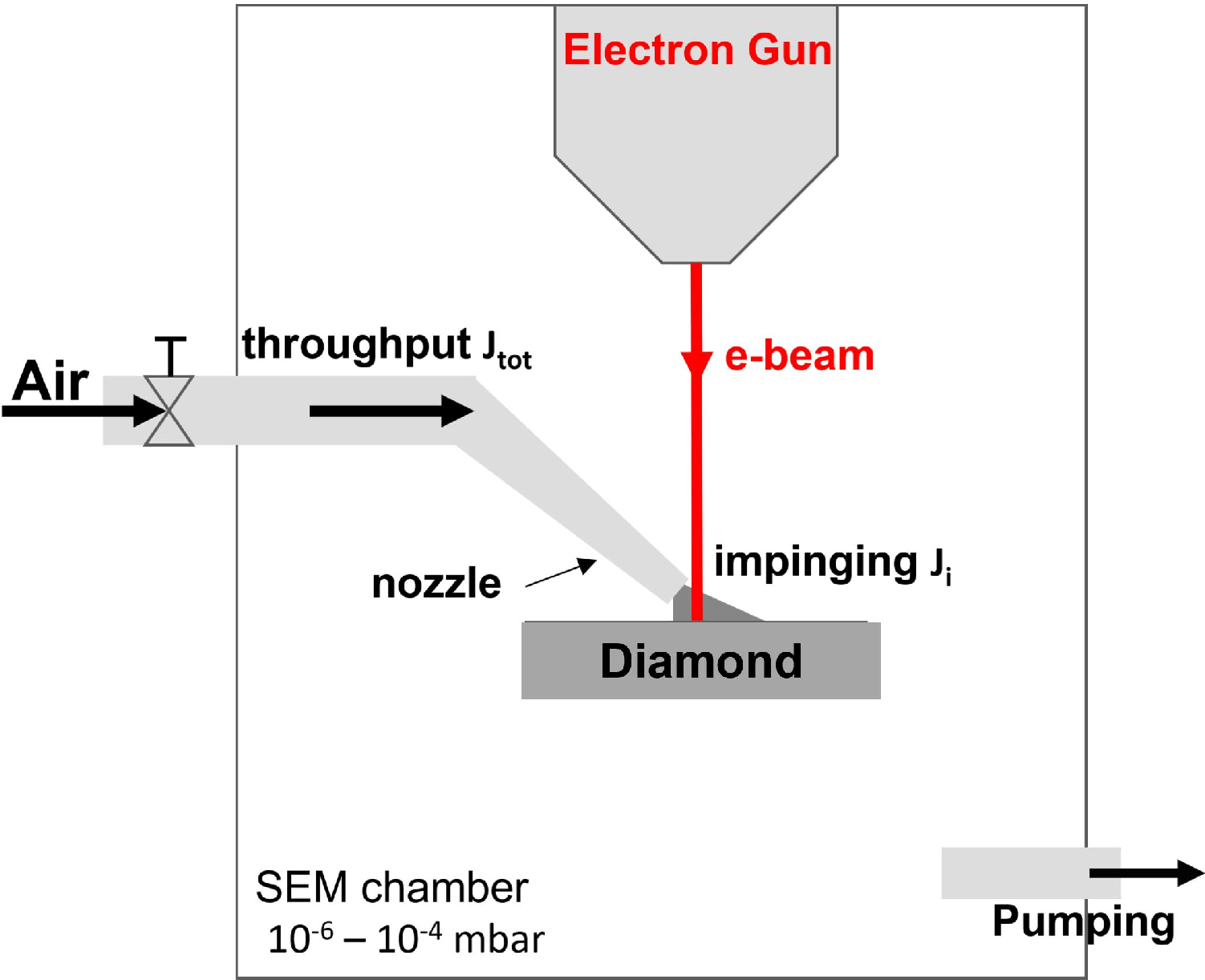
Figure 1: Schematic of the EBIE setup in an SEM chamber where air is introduced via a nozzle to deliver a localized molecular flux, with etching performed by the incident electron beam under controlled pressure.
Secondary Electron–Driven Etching Mechanism
A central finding is that the etch yield is maximized at primary electron (PE) energies of 3 keV and is tightly correlated with the SE emission yield profile. In the 1–10 keV energy range, SE yields are highest at low energies, peaking near 1 keV, then falling as PE energy increases. The etching yield similarly features a peak at 3 keV; no etching is detected at 10 keV. This confirms that SEs rather than primary or backscattered electrons (BSEs) dominate gas dissociation in EBIE for diamond.
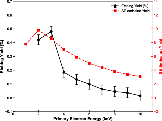
Figure 2: Experimental correlation between diamond etching yield and secondary electron emission yield as a function of primary electron energy highlights the SE-driven dissociation mechanism.
Cross section analysis reveals that SEs (<50 eV) efficiently dissociate O2, N2, and H2O—the principal air components—by maximizing radical generation at $10$–$75$ eV. Oxygen and nitrogen radicals generated thereby chemisorb onto diamond, forming volatile species (CO, CN), enabling material removal. The negligible role of other air constituents (Ar, CO2, CH4) is consistent with their low concentrations.
Spatial Flux Engineering and Resolution
Resolution and pattern fidelity in EBIE are strongly dictated by the spatial distribution of the air molecular flux, governed by the nozzle-to-beam geometry. High impinging flux near the nozzle (low xs) results in sharply localized, deep etching (down to 200 nm lateral size), whereas remote positions (large xs) generate broader, shallower, and more elliptical patterns due to decreased local gas density and increased SE mean free path.
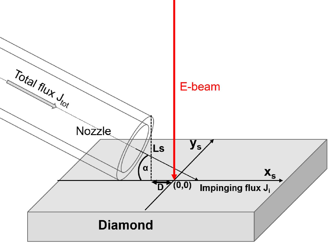
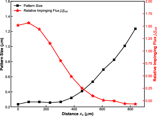
Figure 3: The spatial dependence of etching is modulated by the nozzle-to-beam distance xs, with maximum resolution near the gas nozzle and feature broadening at increased 20.
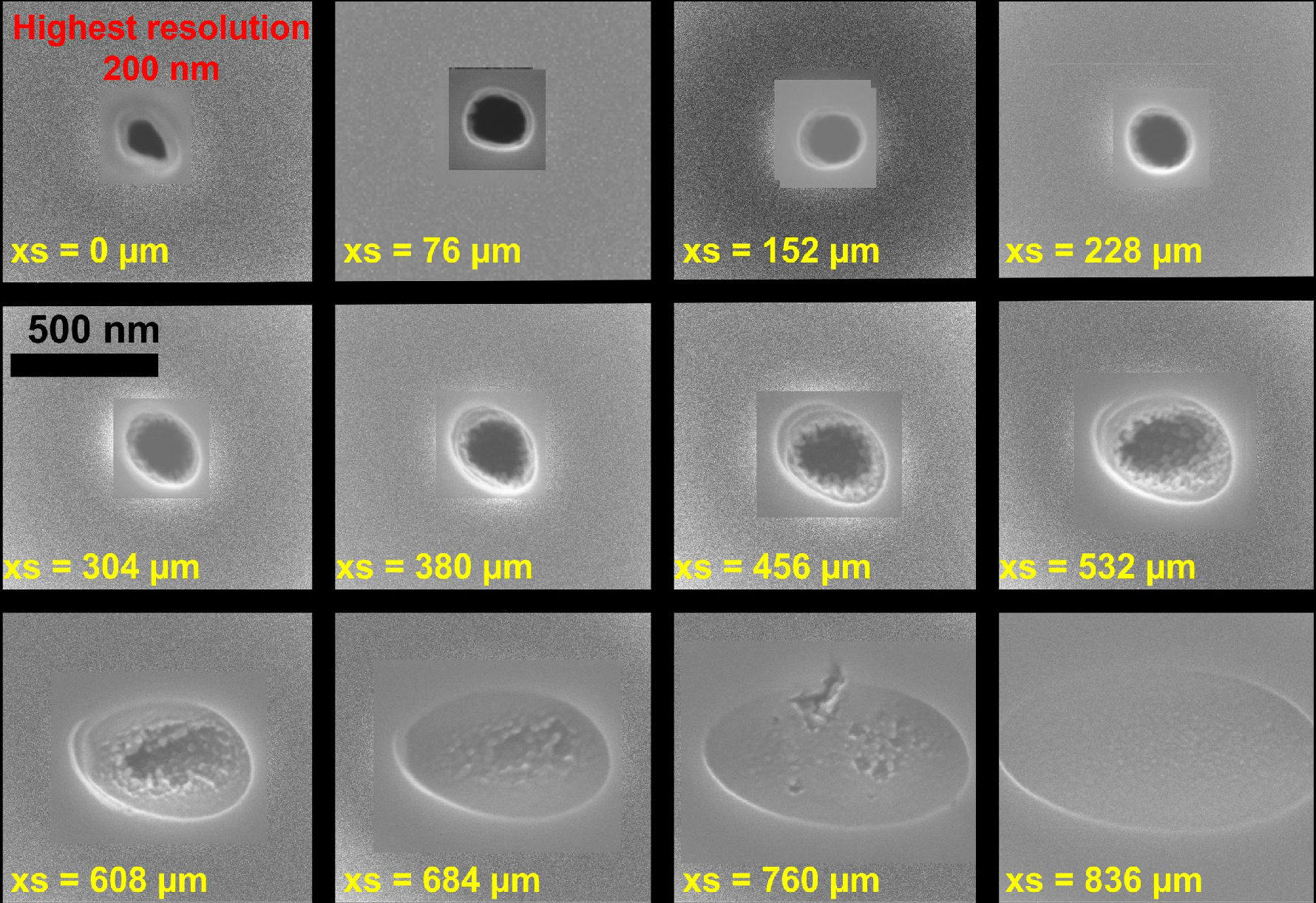
Figure 4: SEM micrographs demonstrate the qualitative evolution of the etch pit shape and size as 21 increases, tracking the reduction in both local gas flux and etching depth.
Dual Regimes: Molecule-Limited and Electron-Limited Etching
The system transitions between molecule-limited and electron-limited regimes, as captured by pressure and current density sweeps. At low chamber pressures, the etching yield increases monotonically with pressure (more available molecules), while at high pressures, the surface saturates and the yield saturates due to limited SE flux.
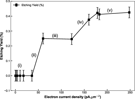
Figure 5: The dependence of etching yield on electron current density reveals two distinct plateau regimes corresponding to successive desorption thresholds for CO and CN surface species.
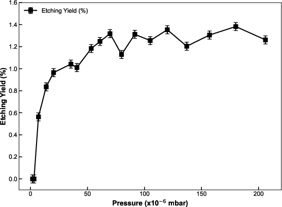
Figure 6: Etching yield as a function of chamber pressure illustrates sharp yield growth in the molecule-limited regime followed by a plateau in the electron-limited regime at higher pressures.
Two clear yield plateaus are also evident versus current density, reflecting the activation of CO desorption (lower energy) at moderate densities and CN desorption (higher energy, requiring higher local heating) at higher densities.
Dwell Time and Temporal Anisotropy
Etching yield demonstrates non-monotonic behavior with scanning dwell time, peaking at 3 μs—a balance point where electron flux and gas availability are jointly optimized. Insufficient or excessive dwell times result in electron- or molecule-limited conditions that degrade efficiency.
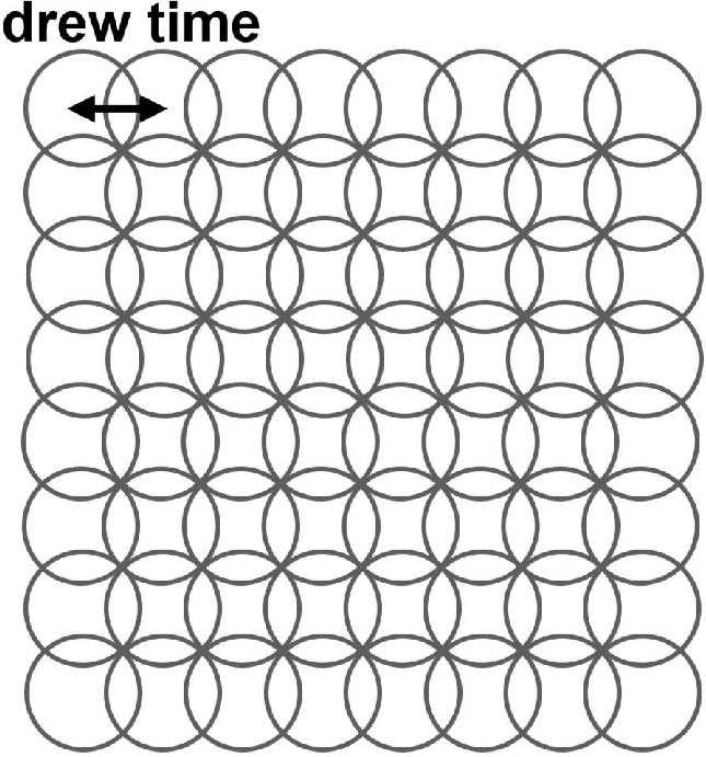
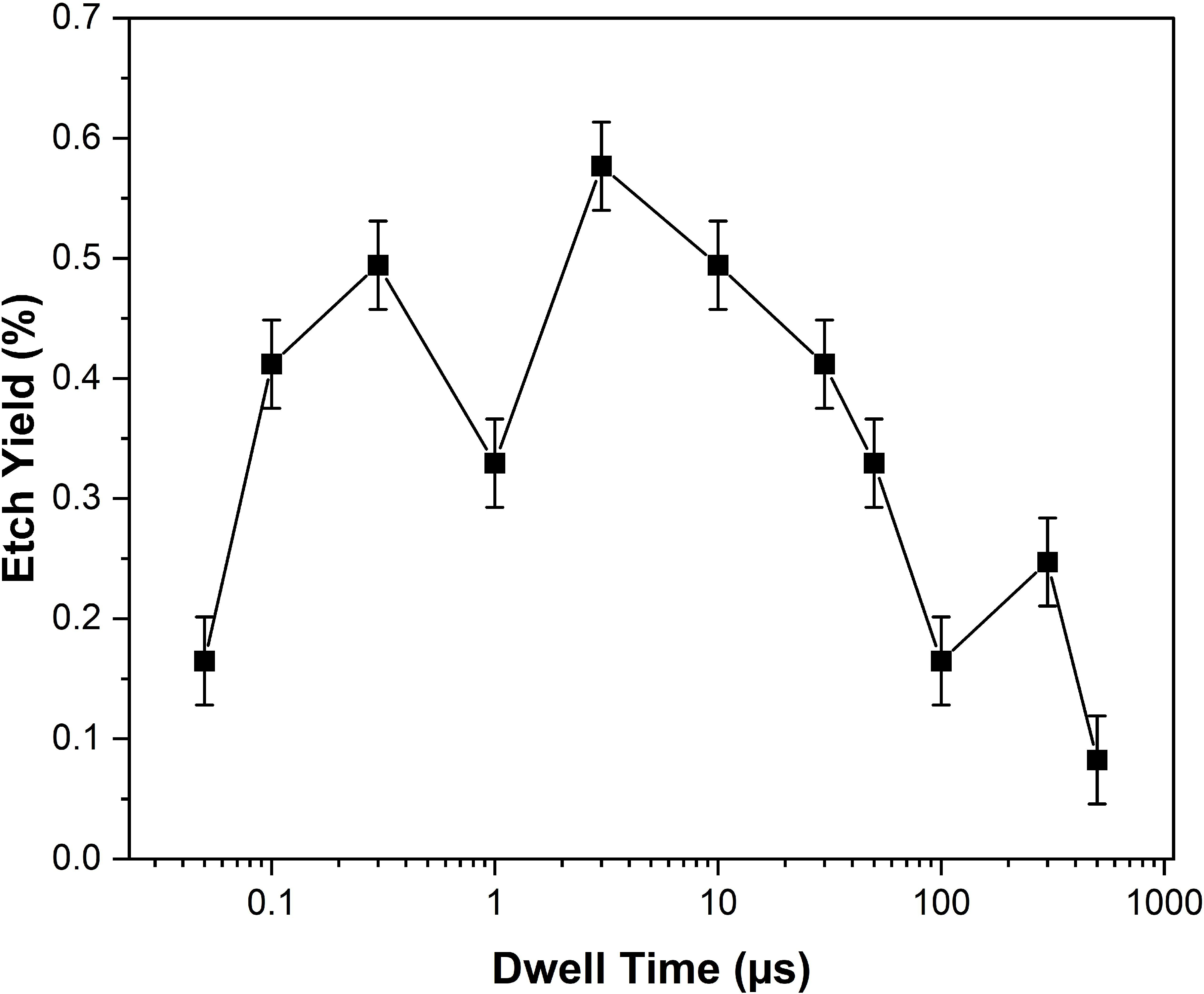
Figure 7: (a) Definition of dwell time and (b) measured etching yield versus dwell time reflect an optimum dwell period where radical generation and desorption are balanced.
Long-term irradiation shows a transition in etched surface morphology. Initially isotropic etching transforms into highly anisotropic, crystallographically selective etching, with (111)-faceted inverse pyramidal pits dominating for exposure times ≥9 min.
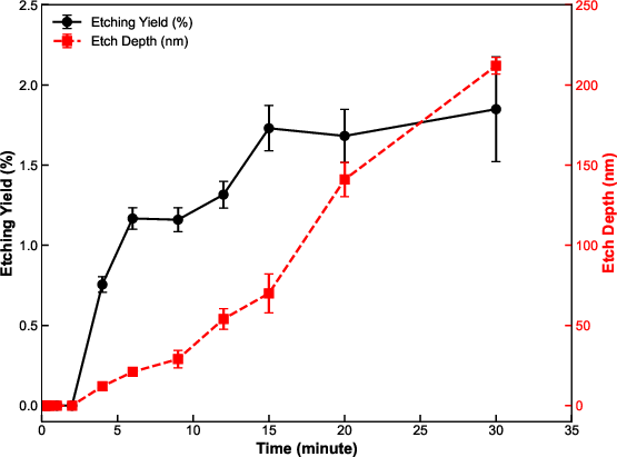
Figure 8: Etching yield and depth as a function of cumulative electron exposure time reveal initial delay, two plateaus, and overall yield enhancement correlated with surface morphological changes.
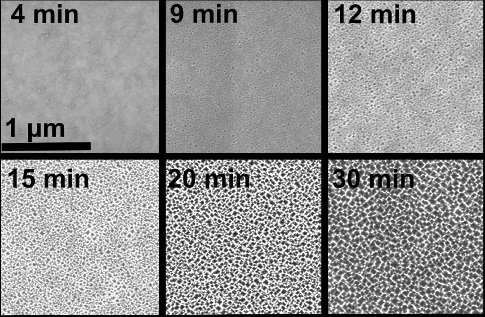
Figure 9: SEM images depict the progression from flat to highly anisotropic surfaces, with elongated (111)-facet pits increasing in number and size at extended exposure times.
This morphological transformation increases the active surface area by ~74% once the surface becomes densely populated with (111) facets, boosting etch yield by up to 60% relative to short exposure times.
Process Mechanistic Summary
The mechanistic sequence for air-based EBIE is:
- Primary electrons: PEs impinge, predominantly generating low-energy SEs.
- Secondary electron scattering: SEs dissociate O22 and N23 near the diamond surface, maximally producing reactive radicals at 10–75 eV.
- Radical adsorption: O and N radicals chemisorb, reacting with surface carbon to form volatile CO/CO24/CN species.
- Desorption: Continued electron irradiation liberates these species, effecting material removal.
- Regime transitions: The rate-limiting step alternates between molecular supply and electron-induced desorption depending on process parameters.
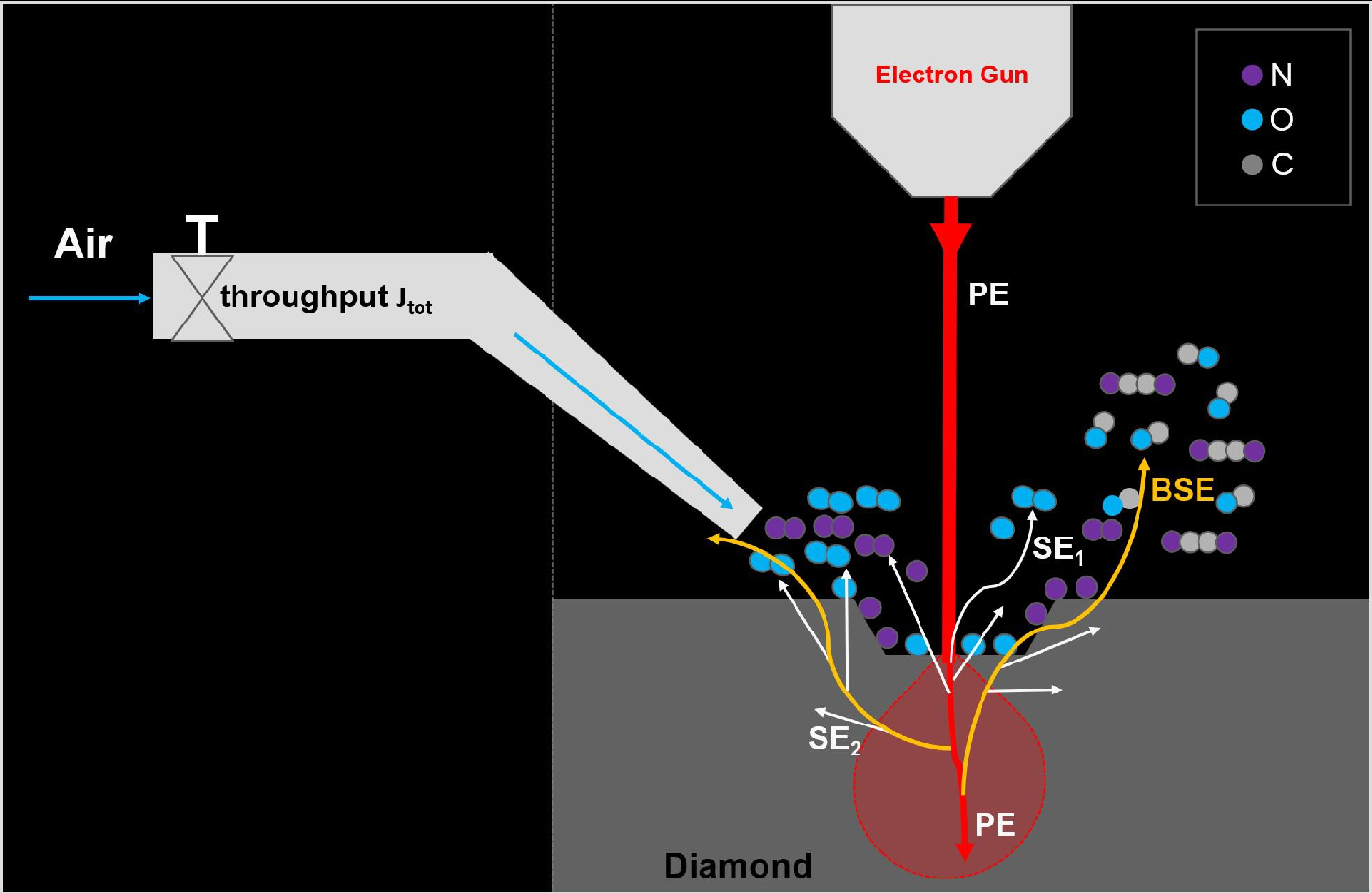
Figure 10: Schematic of the air-based EBIE process, highlighting the cascade of SE-driven gas dissociation, radical-surface chemistry, and product desorption.
Nitrogen's presence in air is implicated in etch anisotropy, promoting the stabilization of (111) facets versus the isotropic etching typical in pure O25 environments.
Practical and Theoretical Implications, Outlook
This air-based, maskless EBIE process is fully compatible with existing SEM infrastructure, allowing direct nanostructuring of diamond with lateral resolution down to 200 nm and maximum depths of 212 nm without lithographic preprocessing or plasma-induced subsurface damage. The technique is especially suited for the fabrication of photonic and quantum devices where surface coherence, minimal dead-layers, and defect management are crucial. The elucidation of the SE-driven mechanism, radical chemistry, and regime mapping provides a foundation to generalize maskless EBIE to other chemically inert materials, including wide-bandgap semiconductors and atomically thin van der Waals crystals.
Conclusion
Maskless EBIE in air enables direct-write, high-resolution, anisotropic etching of diamond via a secondary electron–driven radical mechanism, under process conditions that are accessible to standard SEM platforms. The study delineates key operational regimes, establishes process-structure-property relationships, and provides quantitative guidance for the optimization of current, pressure, dwell time, and spatial nozzle configuration. The deeper mechanistic understanding lays the groundwork for future adaptive nanomanufacturing strategies in quantum materials science and beyond.

