Spin splitting, Kondo correlation and singlet-doublet quantum phase transition in a superconductor-coupled InSb nanosheet quantum dot
Abstract: We realize a superconductor-coupled quantum dot (QD) in an InSb nanosheet, a 2D platform promising for studies of topological superconductivity. The device consists of a superconductor-QD-superconductor junction, where a bottom bilayer gate defines the QD and allows tuning of its coupling to the superconducting leads. The QD exhibits large $g$-factors and strong spin-orbit coupling. Transport measurements reveal Coulomb diamond-shaped differential conductance features with even-odd alternating sizes and pronounced conductance lines associated with the superconducting gap, confirming a few-electron, superconductor-coupled regime. At an odd electron occupation, Kondo signatures emerge, including a zero-bias peak that splits with magnetic field and is logarithmically suppressed at elevated temperatures. We further observe a doublet-singlet quantum phase transition, manifested by a clear change of Andreev bound states from crossing to anticrossing as the coupling strength increases. These results underscore the rich physics of InSb nanosheet QDs and their promise for topological quantum devices.

Paper Prompts
Sign up for free to create and run prompts on this paper using GPT-5.
Top Community Prompts
Explain it Like I'm 14
Plain-language summary of “Spin splitting, Kondo correlation and singlet-doublet quantum phase transition in a superconductor-coupled InSb nanosheet quantum dot”
Overview: What is this paper about?
This paper shows how scientists built a tiny, controllable “electron box” (called a quantum dot) inside a thin sheet of a special material, indium antimonide (InSb). They connected this box to superconductors—materials that can carry electric current with zero resistance at very low temperatures. By carefully measuring how electrons move through this setup, they observed several important quantum effects that are useful for future quantum computers, especially devices that might use “topological” states like Majorana zero modes.
Goals: What did the researchers want to find?
The researchers set out to:
- Make a high-quality quantum dot in a flat (2D) InSb nanosheet and connect it to superconductors.
- Check if this quantum dot shows strong spin behavior (big “g-factors”) and strong spin-orbit coupling, both important for quantum devices.
- Look for the Kondo effect, a quantum phenomenon that boosts electrical conductance at very low voltages and temperatures when there’s an unpaired electron.
- Watch how special states called Andreev bound states change as they tune the connection between the quantum dot and the superconductors, revealing a “phase transition” between different ground states (singlet vs doublet).
Methods: How did they do it (in simple terms)?
Think of a quantum dot as a tiny room that can trap one or a few electrons. The team:
- Built a “two-layer gate” system under a thin InSb sheet. These gates act like knobs to:
- Set the dot’s energy level (which determines how many electrons want to sit in the room).
- Control the barriers on the left and right (how easily electrons can enter or leave).
- Shape the dot’s walls (how strongly the dot confines electrons).
- Placed superconducting metal contacts (made of titanium/aluminum) on top of the nanosheet to connect the dot to superconducting leads.
- Cooled the device to extremely low temperatures (around 25 millikelvin) so superconductivity and delicate quantum effects could appear.
- Measured how easily current flows through the dot while changing:
- Voltage across the device (source-drain bias)
- Gate voltages (to tune dot energy and couplings)
- Magnetic field (to split spin states)
- Temperature (to see how quantum effects fade as things heat up)
If you imagine plotting the results, the graphs show “diamond-shaped” patterns (called Coulomb diamonds). These diamonds tell you when electrons can or can’t enter the dot—like a turnstile letting one electron through at a time. The shapes and sizes of the diamonds reveal the dot’s energy structure and whether it has an even or odd number of electrons.
A few key terms explained with everyday analogies:
- Spin: An electron’s spin is like a tiny arrow that can point “up” or “down.” A magnetic field can split the energy of these spins apart (spin splitting).
- g-factor: Measures how strongly an electron’s spin reacts to a magnetic field. A large g-factor means spins split more for the same field.
- Spin-orbit coupling: The electron’s spin and motion are linked, like a dancer whose spin depends on their path across the floor. This can mix energy levels.
- Kondo effect: If the dot holds one lonely electron, the electrons in the leads “team up” with it at low temperature, making it easier for current to flow right at zero voltage—like a crowd gathering around a performer, making a path through the room.
- Andreev bound states (ABS): Special energy states inside the dot caused by the superconductor, where electrons and holes pair up in a delicate way due to the superconducting leads.
- Singlet vs doublet: Singlet means electrons are paired (total spin 0), doublet means there’s one unpaired electron (spin 1/2). Switching between these is a “quantum phase transition.”
Main findings: What did they discover and why is it important?
Here are the most important results the team saw:
- Working 2D device with few electrons
- The dot showed clear Coulomb diamonds with alternating sizes for even and odd electron counts. That’s a sign they reached the few-electron regime and had good control.
- Large g-factors and strong spin-orbit coupling
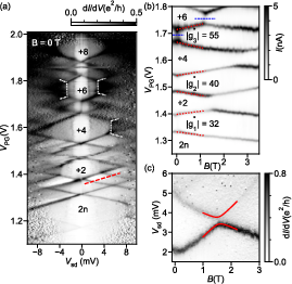
- Different energy levels had big g-factors (about 32, 40, and 55), meaning spins split strongly in magnetic fields—great for spin-based control.
- They observed level mixing due to spin-orbit coupling and estimated a spin-orbit energy around 186 micro–electronvolts. Strong spin-orbit coupling is key for creating topological states.
- Kondo effect in the odd-electron state
- At zero magnetic field, they saw a strong conductance peak at zero bias inside the odd-electron diamond—classic Kondo behavior.
- Applying a magnetic field split this peak into two, as expected when spin degeneracy is lifted.
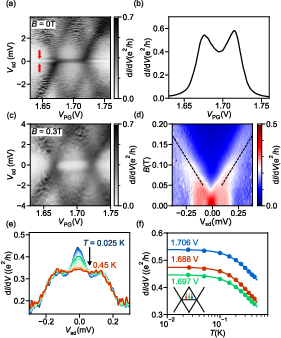
- Warming the device gradually suppressed the Kondo peak, and by fitting the temperature dependence, they found Kondo temperatures around 0.94–1.06 K, highest near the points where the dot is about to gain or lose an electron.
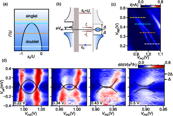
- Singlet–doublet quantum phase transition in Andreev bound states
- By increasing how strongly the dot couples to one superconducting lead, the ABS patterns changed:
- At weak coupling, the ABS resonances formed loops that crossed zero energy—signaling a transition between doublet (unpaired) and singlet (paired) ground states.
- At stronger coupling, those crossings turned into “anticrossings” (they avoid crossing), showing the system settled into a different ground state.
- This crossing-to-anticrossing change is direct evidence of the singlet–doublet phase transition controlled by the coupling strength.
- Soft superconducting gap observed
- The device’s superconducting leads sometimes allowed a small number of “quasiparticles” near zero energy (a “soft gap”), likely due to interface processing steps. The authors note that future devices with cleaner, epitaxial superconductor contacts could produce a “hard gap,” improving performance.
Why it matters: Implications and future impact
This work shows that a flat, 2D InSb platform can host a high-quality, superconductor-coupled quantum dot with strong spin properties and rich quantum behavior. That’s important because:
- 2D designs can be arranged into complex networks needed for building topological quantum computers.
- Strong spin-orbit coupling and large g-factors are crucial ingredients for creating and controlling exotic states like Majorana zero modes—promising building blocks for robust quantum bits.
- The ability to tune the singlet–doublet transition and to clearly see Kondo physics shows precise control over electron states, which is vital for reliable readout and manipulation in quantum devices.
- With improved superconductor–semiconductor interfaces (to achieve a hard gap), these devices could become powerful, scalable components for future topological quantum technologies.
In short, the paper demonstrates a versatile 2D platform that captures many of the quantum effects needed for next-generation quantum computing, and it points to clear routes for making these devices even better.
Knowledge Gaps
Unresolved knowledge gaps, limitations, and open questions
Below is a consolidated list of concrete gaps and open questions that remain after this study and can guide targeted follow-up work:
- Hard-gap absence and ABS interpretation: The induced superconducting gap is soft, complicating unambiguous identification of zero-energy Andreev bound state (ABS) crossings versus “mirage” features caused by finite subgap density of states. How do the spectra change with hard-gap contacts (e.g., in situ epitaxial Al) or with a normal-metal probe to decouple probe-induced artifacts?
- Quantitative extraction of device energy scales: The coupling is only qualitatively tuned via ; values of , , , and are not quantitatively extracted from the ABS spectra. Can numerical fits (e.g., Anderson impurity model/NRG) to bias spectroscopy provide self-consistent parameter sets and their gate dependence?
- Missing phase control and 0–π determination: The phase difference between superconducting leads is not controlled, and no current-phase relation is measured. Can a SQUID geometry or phase-bias device be implemented to directly map the -dispersion of ABSs and identify 0–π transitions unambiguously?
- No direct Josephson supercurrent characterization: The study does not report supercurrent, , or its gate/temperature dependence across the singlet–doublet transition. How does evolve versus , , , and magnetic field, and does it exhibit a 0–π sign change consistent with the ABS spectroscopy?
- Kondo–superconductivity interplay not mapped versus : Although K is extracted and is inferred from conductance onsets, the phase boundary governed by is not quantified. Can systematic tuning of (via field, superconductor choice, or thickness) map the singlet–doublet boundary and test universal scaling?
- Angular anisotropy of -factor and spin–orbit field unresolved: Only an in-plane magnetic field is used; the full -tensor and its anisotropy are not characterized. How do and ABS Zeeman shifts vary with 3D field orientation, and how does this correlate with the spin–orbit field direction in the nanosheet?
- Gate tunability of spin–orbit coupling not demonstrated: A single spin–orbit anticrossing (eV) is extracted, but Rashba tuning via vertical electric field is not explored. Can be tuned with gate voltages (PG/CG) and how does this affect -factor fluctuations and ABS spectra?
- Origin of extra finite-bias conductance lines uncertain: Features attributed to “additional transport channels in the lead regions” or inelastic cotunneling are not verified. Can these be disambiguated by (i) driving the device normal, (ii) altering contact depletion with barrier gates, or (iii) comparing to simulations of lead subband thresholds?
- Soft gap origin not isolated experimentally: While ammonium sulfide/Ar plasma processing is cited as a possible cause, no comparative devices with different surface preparations are shown. Do devices with epitaxial Al or alternative interface cleaning exhibit hard gaps and sharper ABS features?
- Reproducibility across devices and cooldowns not provided: The results are from a single device/configuration. What is the device-to-device variability in , , , , , , and ABS crossing behavior?
- Temperature dependence of not measured: The Kondo scaling analysis assumes is temperature-independent up to 0.45 K. Can independent tunneling spectroscopy quantify to validate the applicability of the empirical Kondo scaling?
- Magnetic-field dependence of ABS not mapped: Zeeman splitting and evolution of Yu–Shiba–Rusinov-like states with are not investigated. How do ABS energies split/shift with in odd-occupancy valleys, and do they delineate the singlet–doublet phase boundary?
- Asymmetric vs symmetric coupling effects unaddressed: The left lead is used as a weakly coupled probe (near pinch-off), and only is tuned. How do ABS and Kondo features evolve when tuning both barriers to explore symmetric/asymmetric coupling regimes?
- Quasiparticle poisoning and parity lifetimes uncharacterized: The soft gap suggests residual quasiparticles, but parity stability is not measured. What are the parity lifetimes and subgap quasiparticle densities, and how do they impact ABS linewidths and zero-bias features?
- High-frequency dynamics of ABSs (coherence/relaxation) unexplored: No microwave spectroscopy is performed. What are ABS relaxation and dephasing times, and how do they change across the singlet–doublet transition and with ?
- Independent determination and calibration of : The gap scale is inferred from transport features near ±0.2 mV, but not rigorously established (e.g., 2/e vs /e threshold ambiguity). Can a dedicated tunnel probe or normal-metal junction provide an unambiguous value and hardness?
- Role of 2D confinement and dot geometry not quantified: Only the average level spacing is reported; the dot’s shape, size, and confinement anisotropy are not extracted. Can excited-state spectroscopy along orthogonal gates and electrostatic modeling link level spacings to geometric confinement?
- Cross-capacitance and potential landscape not mapped: The influence of unused gates (biased at −0.5 V) and gate cross-couplings on the dot potential is not quantified. Can a capacitance matrix be extracted to better control/interpret and tunneling barriers?
- Electron temperature calibration absent: Kondo and ABS linewidth analyses require accurate electron temperature, but no independent thermometry is shown. Can Coulomb-peak thermometry or noise-based methods confirm ?
- MAR vs ABS contributions to subgap conductance not disentangled: Multiple Andreev reflection (MAR) is cited as background, but subharmonic gap structures are not analyzed. Can transparency-dependent measurements identify MAR onsets and separate them from ABS resonances?
- Nonlinear Kondo scaling (bias vs temperature) not tested: Only linear-response Kondo scaling with is reported. Does differential conductance collapse onto the universal scaling function versus across the odd diamond?
- Orbital effects and higher-level structure not explored: Beyond a single spin–orbit anticrossing, a comprehensive mapping of orbital excitations vs is absent. Can higher-field magnetospectroscopy distinguish orbital vs spin contributions to level shifts?
- Charge noise and telegraph noise impact on linewidths unresolved: Broadening of ABS/Kondo features and potential charge fluctuations are not quantified. Can time-resolved conductance or noise spectroscopy assess charge stability and its effect on spectroscopy?
- Path to topological regimes not demonstrated: While the platform is positioned for topological physics, no measurements approach the Majorana regime (e.g., phase-biased multi-junctions, chains, or robust zero-bias modes). What device modifications (phase control, multiterminal junctions, larger induced gaps) are required to reach and diagnose topological phases?
- Device architecture scalability not evaluated: The bilayer gate approach is promising, but its yield, uniformity, and compatibility with complex geometries are not assessed. Can arrays of dots/junctions be fabricated with consistent parameters for scalable topological circuits?
Glossary
- addition energy: The energy required to add an extra electron to a quantum dot level, including magnetic-field effects. "the single-particle addition energy evolves as "
- Andreev bound states (ABSs): Subgap bound states formed by coherent Andreev reflections in a superconductor–quantum-dot hybrid. "a transition of Andreev bound states from crossing to anticrossing as the coupling strength increases"
- Andreev levels: The discrete energy levels of Andreev bound states within the superconducting gap. "giving rise to Andreev levels ."
- anticrossing: An avoided energy-level crossing caused by coupling or hybridization between states. "an anticrossing develops between the spin-down ground state and the spin-up excited state"
- atomic layer deposition (ALD): A thin-film growth technique that deposits materials one atomic layer at a time. "and was capped with a 10-nm-thick AlO film grown via atomic layer deposition."
- ballistic transport: Electron transport with negligible scattering over the device length. "In 2D InSb-based Josephson junctions, ballistic transport has been observed"
- Bohr magneton: A physical constant that sets the scale of the electron’s magnetic moment. "(with the Bohr magneton)"
- Bogoliubov-type superposition: A superconducting state that is a coherent mixture of different particle-number configurations. "The latter arises from a Bogoliubov-type superposition of the QD's empty state and two-electron state ."
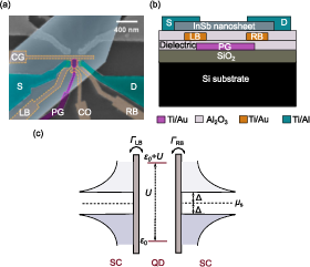
- charge stability diagram: A map of current or conductance versus gate voltages that reveals charge states of a quantum dot. "Figure~\ref{fig4}c shows the charge stability diagram of the superconductor-coupled QD"
- charge-degeneracy point: A gate-voltage condition where two adjacent charge states of the dot are energetically degenerate. "with the peaks occurring near the charge-degeneracy points"
- charging energy (U): The Coulomb energy cost to add one electron to a quantum dot. "we further deduce an average charging energy = 4.4~meV"
- Coulomb blockade: Suppression of electron transport due to quantization of charge and charging energy in small conductors. "a hallmark of electron transport through a few-electron QD in the Coulomb blockade regime."
- Coulomb diamond: Diamond-shaped regions in bias–gate maps where transport is blocked by Coulomb interactions. "Coulomb diamond-shaped differential conductance features with even-odd alternating sizes"
- differential conductance: The derivative dI/dV of current with respect to voltage, used to reveal spectroscopic features. "Differential conductance d/d as a function of source-drain bias $V_{\text{sd}$ and plunger gate voltage $V_{\text{PG}$"
- dilution refrigerator: A cryogenic system reaching millikelvin temperatures using He-3/He-4 mixtures. "All measurements were conducted in a dilution refrigerator with a base temperature of 25 mK"
- electron effective mass: The band-structure-modified inertial mass of an electron in a solid. "including a small electron effective mass"
- electron-beam lithography (EBL): A nanofabrication method that uses a focused electron beam to pattern resist. "were fabricated on the InSb nanosheet using standard electron-beam lithography"
- g-factor (effective): A dimensionless parameter characterizing the Zeeman splitting of electronic spin states in a material. "we extract an effective -factor of 41"
- hard superconducting gap: A superconducting gap with negligible subgap density of states. "induce hard superconducting gaps in nanowire and quantum well systems"
- inelastic cotunneling: Second-order tunneling through a Coulomb-blockaded dot accompanied by energy exchange to excitations. "the onset of inelastic cotunneling"
- Josephson junction: A weak link between superconductors supporting coherent pair tunneling and supercurrent. "We next investigate singlet-doublet phase transitions in the nanosheet QD-based Josephson junctions."
- Kitaev chain: A 1D topological superconducting model supporting Majorana zero modes at its ends. "Majorana zero modes in artificial Kitaev chains"
- Kondo effect: Enhanced low-temperature conductance due to many-body screening of a localized spin by conduction electrons. "This ridge occurs at the spin degeneracy point ... and represents a hallmark of the spin-1/2 Kondo effect"
- Kondo ridge: A gate-voltage–extended zero-bias conductance peak associated with the Kondo effect in a Coulomb diamond. "a zero-field Kondo ridge that splits as the magnetic field increases"
- Kondo temperature (): The characteristic temperature scale at which Kondo correlations emerge. "Best fitting to the data yields K."
- lever arm: The conversion factor between gate voltage and energy shift of a quantum dot level. "The average voltage-to-energy conversion factor (lever arm) = 0.08"
- Majorana zero modes: Zero-energy quasiparticle excitations in topological superconductors with non-Abelian statistics. "Majorana zero modes in artificial Kitaev chains"
- molecular beam epitaxy (MBE): An epitaxial growth technique for high-purity, crystalline semiconductor layers. "High-quality InSb nanosheets are grown by molecular beam epitaxy (MBE)"
- multiple Andreev reflection: Subgap transport involving successive Andreev reflections at superconducting interfaces under finite bias. "with ABSs and/or multiple Andreev reflection processes contributing to a finite conductance"
- multiterminal Josephson junction: A Josephson device with more than two superconducting leads allowing complex phase control. "and multiterminal Josephson junctions"
- parity (fermionic parity): The evenness or oddness of the total number of fermions, relevant to superconducting ground states. "a spin doublet (, fermionic odd parity) ... and a spin singlet (, fermionic even parity)"
- pinch-off: The gate condition where a conducting channel is fully depleted and current is minimized. "with $V_{\text{LB}$ fixed near pinch-off at ~V."
- plunger gate (PG): A gate electrode that tunes the electrochemical potential of a quantum dot. "the plunger gate (PG) tunes the electrochemical potential () of the QD"
- proximity-induced superconductivity: Superconducting correlations induced in a normal material via contact with a superconductor. "proximity-induced superconductivity has been extensively explored"
- quantum phase transition (singlet–doublet): A zero-temperature transition between distinct many-body ground states (singlet and doublet) tuned by coupling or gate. "A singletâdoublet quantum phase transition is expected only in the regime "
- quantum point contact (QPC): A narrow, gate-defined constriction showing quantized conductance in units of 2e2/h. "including quantum point contacts and quantum dots"
- quasiparticle: An elementary excitation in a superconductor behaving like a particle, e.g., Bogoliubov quasiparticles. "two horizontal differential conductance features are observed ... correspond to a superconducting gap, signaling the onset of direct quasiparticle tunneling"
- soft gap (soft superconducting gap): A superconducting gap with residual subgap density of states due to imperfections. "A soft induced gap in the left probe is taken into account, resulting in a finite quasiparticle density of states near the Fermi level."
- spin–orbit coupling: Interaction between a particle’s spin and its motion in an electric field, leading to spin-dependent band structure. "The QD exhibits large -factors and strong spin-orbit coupling."
- spin–orbit splitting (): Energy splitting between states due to spin–orbit coupling. "yields a spinâorbit splitting of $\Delta_{\text{SO} = 186~\mu\text{eV}$"
- tunnel coupling (): The hybridization strength between a quantum dot and its leads, setting level broadening. "modulate tunnel couplings between the QD and SCs ($\Gamma_{\text{LB}$ and $\Gamma_{\text{RB}$, respectively)"
- voltage bias spectroscopy: Measuring differential conductance versus bias to map subgap states like ABSs. "enabling voltage bias spectroscopy of ABSs across different coupling regimes."
- Zeeman effect: Magnetic-field-induced splitting of spin-degenerate energy levels. "split via the Zeeman effect"
- Zeeman splitting: The energy difference between spin states in a magnetic field proportional to . "is the Zeeman splitting energy of the -th single-particle level"
Practical Applications
Immediate Applications
- Bold: Planar InSb nanosheet QD test vehicle for hybrid-superconductor device R&D
- What it does: Provides a reproducible, gate-tunable platform to study Coulomb blockade, Kondo physics, Andreev bound states (ABS), and singlet–doublet phase transitions in 2D architectures—key for screening materials, interfaces, and layouts before scaling to complex topological circuits.
- Sectors: Semiconductor fabrication (quantum foundries), quantum computing hardware, academic research labs, metrology.
- Tools/Products/Workflows:
- Bilayer fine-gate underlayer design kit for defining QDs while minimizing processing on the nanosheet.
- Process recipes for nanosheet transfer, surface cleaning (NH4)2Sx + mild Ar plasma, and Ti/Al deposition.
- Measurement workflows for Coulomb diamonds, g-factor extraction, ΔSO fitting, and ABS spectroscopy.
- Assumptions/Dependencies: Availability of MBE-grown InSb nanosheets; dilution refrigeration (≤50 mK), in-plane magnetic field; interface control; yield of nanosheet transfer and alignment.
- Bold: ABS spectroscopy as a diagnostic for interface quality and coupling optimization
- What it does: Uses gate-tunable ABS crossing/anticrossing to map coupling strength Γ and identify soft-gap vs hard-gap behavior; enables rapid feedback on interface treatments and superconductor stack choices.
- Sectors: Process metrology, superconducting electronics, quantum foundries.
- Tools/Products/Workflows: “ABS probe” device geometry (probe SC near pinch-off + strongly coupled SC) and voltage-bias spectroscopy scripts; QC dashboards for gap hardness and Γ-tuning curves.
- Assumptions/Dependencies: A soft gap is acceptable for diagnosis; for deployment in protected qubits, transition to epitaxial Al or other hard-gap stacks is needed.
- Bold: Gate-tunable 0–π Josephson element prototyping via singlet–doublet transitions
- What it does: Demonstrates a controllable transition of ABS from crossing to anticrossing, enabling proof-of-principle 0–π switching elements in test circuits and SQUID loops.
- Sectors: Superconducting circuit design, quantum device prototyping.
- Tools/Products/Workflows: Gate maps to target the odd-occupancy window (−U < ε0 < 0), Γ-tuning via barrier gates, integration into phase-biasable loops for switching demonstrations.
- Assumptions/Dependencies: Requires maintaining ABS coherence and stable phase bias; current device exhibits a soft gap which limits coherence; low magnetic field operation preferred when integrating with flux-based circuits.
- Bold: Kondo-based cryogenic thermometry and spectroscopic calibration
- What it does: Uses the temperature scaling of the zero-bias Kondo ridge (G(T) fit with known s-parameter) to calibrate electron temperature in dilution fridges between ~50 mK and ~1 K, and to benchmark magnetic-field alignment via Zeeman splitting.
- Sectors: Cryogenic instrumentation, metrology, academic labs.
- Tools/Products/Workflows: Calibration scripts extracting TK from conductance vs temperature and g* from field-splitting; integration into cryostat acceptance tests.
- Assumptions/Dependencies: Requires an odd-occupancy Coulomb diamond and suppressed superconductivity (or accounting for subgap background); stable gate operation over thermal cycles.
- Bold: Parameter-extraction software and ML-assisted autotuning for planar QD–SC devices
- What it does: Automates detection of Coulomb diamonds, even–odd alternation, Kondo ridges, and ABS loops to extract U, α (lever arm), ΔSO, g-factors, and Γ; accelerates device bring-up and reproducibility across wafers.
- Sectors: Software for quantum labs, EDA for quantum devices, test engineering.
- Tools/Products/Workflows: Python package/notebooks for data ingestion and fitting; ML classifiers for “odd/even” charge states and “crossing/anticrossing” ABS patterns; lab-in-the-loop optimization of gate voltages.
- Assumptions/Dependencies: Access to labeled datasets; consistent measurement metadata; cross-device variability handled by transfer learning.
- Bold: Process guidelines to minimize semiconductor–superconductor interface degradation
- What it does: Codifies “minimal top-surface processing” workflows (underlayer gates, single-step SC deposition post-transfer) to improve interface transparency and device yield.
- Sectors: Quantum foundries, materials processing.
- Tools/Products/Workflows: Standard operating procedures for nanosheet transfer, timing between oxide removal and SC deposition, acceptable plasma parameters, dielectric stack sequencing.
- Assumptions/Dependencies: Trade-offs between cleanliness and damage (e.g., plasma conditions) must be tuned per toolset; eventual migration to in-situ epitaxial SC for hard gaps.
- Bold: Education and training modules on correlated transport and proximitized semiconductors
- What it does: Provides a contemporary experimental basis for advanced lab courses on Kondo physics, spin–orbit coupling, and ABS in hybrid nanostructures.
- Sectors: Higher education, workforce development.
- Tools/Products/Workflows: Virtual labs and curated datasets for remote analysis; step-by-step parameter extraction exercises.
- Assumptions/Dependencies: Physical replication requires cryogenics; virtual modules can deploy immediately.
Long-Term Applications
- Bold: Planar topological qubits in 2D InSb networks with QD-based readout and control
- What it could enable: Scalable, phase-controllable planar architectures hosting Majorana zero modes (MZMs), with QDs used for parity readout and tunnel-barrier tuning; multi-island networks for braiding and error-protected operations.
- Sectors: Quantum computing hardware, advanced fabrication.
- Tools/Products/Workflows: Epitaxial Al/InSb heterostructures for hard gaps; multi-terminal Josephson junctions with phase control; QD-assisted MZM readout modules; cryo-CMOS for dense gate control.
- Assumptions/Dependencies: Requires hard induced gaps, low disorder, reproducible Γ control, quantifiable topological gap, system-level error rates competitive with alternatives; substantial cryogenic and control electronics advances.
- Bold: Andreev/ABS- and 0–π-based qubits integrated into superconducting circuits
- What it could enable: Qubits leveraging spinful ABS or parity-protected 0–π states with gate-tunable spectra; potential resilience to some noise channels and compact footprints.
- Sectors: Superconducting quantum hardware, microwave engineering.
- Tools/Products/Workflows: Coherent coupling of ABS to resonators, microwave spectroscopy, Hamiltonian engineering via gates and phase; compact models for circuit design.
- Assumptions/Dependencies: Demonstration of coherence times, controllability, and noise immunity; elimination of soft gaps; materials and interface uniformity across arrays.
- Bold: Multiterminal Josephson junctions for synthetic topological band structures
- What it could enable: Phase-tuned topological superconductivity and nontrivial band topology (e.g., quantized transconductance) in planar networks; reconfigurable “topological chips.”
- Sectors: Quantum devices, metrology, fundamental physics.
- Tools/Products/Workflows: On-chip phase biasing, vector-magnet integration, precision phase-control electronics; wafer-scale layouts of multi-terminal junction meshes.
- Assumptions/Dependencies: High-yield multi-terminal junctions, stable phase coherence across networks, accurate phase calibration at scale.
- Bold: Spin–orbit and g-factor engineering for fast, hybrid spin–superconducting qubits
- What it could enable: Rapid electrical control via strong spin–orbit coupling in proximitized 2D semiconductors, combining long-lived spin states with superconducting readout.
- Sectors: Quantum computing hardware, materials engineering.
- Tools/Products/Workflows: Gate stacks for local SO tuning; co-integration with superconducting resonators; fast voltage-pulse sequencing.
- Assumptions/Dependencies: Uniform device-to-device SO strength; minimal spin-flip noise from interfaces; robust control/readout fidelities.
- Bold: Quantum-limited sensors based on ABS/Kondo resonances
- What it could enable: Ultra-sensitive detectors for magnetic fields, charge noise, or microwave photons exploiting sharp spectral features and parity sensitivity of ABS or Kondo resonances.
- Sectors: Sensing and instrumentation, astrophysics, materials characterization.
- Tools/Products/Workflows: Coupling to high-Q cavities, impedance-engineered readout, noise-mitigation packaging.
- Assumptions/Dependencies: Requires stable, hard gaps and long-lived bound states; careful thermalization; mitigation of quasiparticle poisoning.
- Bold: Foundry-scale PDKs and compact models for planar InSb–superconductor devices
- What it could enable: Design automation for hybrid quantum chips (layout, LVS/DRC, parameterized cells), compact models capturing ABS spectra and Γ-tuning for circuit simulators.
- Sectors: EDA for quantum, semiconductor foundries, design services.
- Tools/Products/Workflows: Process design kits (PDKs) with statistical variability, model cards for ABS/0–π elements, verification flows for cryo environments.
- Assumptions/Dependencies: Process standardization across fabs, IP agreements, correlation between model parameters and measured device statistics.
- Bold: Supply-chain and standards development for hybrid semiconductor–superconductor platforms
- What it could enable: Consistent quality of InSb nanosheets/wells, standardized “gap hardness” and interface-transparency metrics, and safety/environmental protocols for surface chemistries.
- Sectors: Policy, industry consortia, standards bodies.
- Tools/Products/Workflows: Round-robin benchmarking, reference devices and datasets, certification criteria for hard-gap processes.
- Assumptions/Dependencies: Pre-competitive collaboration, data sharing, alignment with export-control and dual-use regulations.
- Bold: Automated nanosheet handling and 3D integration in manufacturing
- What it could enable: Robotic placement and alignment of nanosheets over buried gates, 3D integration with cryo-CMOS, and TSV-based fan-out for dense control wiring.
- Sectors: Advanced packaging, robotics, semiconductor manufacturing.
- Tools/Products/Workflows: Pick-and-place robotics with nanoscale alignment; bonding compatible with cryogenic operation; reliability testing under thermal cycling.
- Assumptions/Dependencies: Mechanical robustness of nanosheets; yield and throughput to be proven for volume production.
Notes on cross-cutting assumptions and dependencies
- Cryogenic operation: All near-term uses require dilution refrigeration and stable magnetic fields; energy and infrastructure costs are nontrivial.
- Interface quality: Transition from soft to hard induced gaps (e.g., via in-situ epitaxial Al) is pivotal for coherent devices; current Ti/Al with ex-situ cleaning is adequate for diagnostics but not for fault-tolerant qubits.
- Materials reproducibility: Uniform g-factors and spin–orbit parameters across devices remain an active challenge; g-factor fluctuations observed here inform design margins.
- Noise and poisoning: Quasiparticle poisoning and charge noise must be mitigated for long-term qubit applications; packaging and shielding co-design is required.
- Scalability: Bilayer-gate underlays and nanosheet transfer are promising but will need automation and statistical process control for wafer-level scaling.
Collections
Sign up for free to add this paper to one or more collections.