- The paper proposes an ADC-less TDC-based CiM architecture that digitizes MAC operations in SRAM, drastically reducing power and area consumption.
- It integrates a custom 4-bit TDC with pulse-shrinking delay elements and a resonant energy-recycling write driver to enable robust and linear MAC digitization.
- Experimental benchmarks demonstrate up to 8× energy reduction with 320 GOPS throughput and minimal accuracy loss, supporting flexible weight-stationary mapping across CNNs.
TDC-Based Resonant Compute-in-Memory for INT8 CNNs with Layer-Optimized SRAM Mapping
Introduction and Motivation
The paper addresses the major limitations of traditional compute-in-memory (CiM) architectures for neural network (NN) acceleration, particularly targeting convolutional neural networks (CNNs) with INT8 quantization. Conventional CiM architectures typically incorporate analog-to-digital converters (ADCs) for MAC operation readout, which introduce significant area, power, and non-linearity penalties—accounting for nearly 59% of total CiM power consumption (Figure 1).
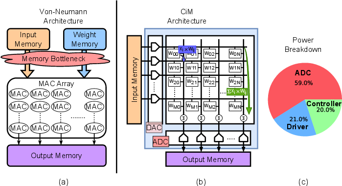
Figure 1: Conventional architectures suffer from memory movement bottlenecks and high ADC power, motivating ADC-less analog MAC digitization.
To circumvent these constraints, the authors propose an ADC-less, resonant time-domain CiM (TDC-CiM) architecture. This approach digitizes analog multiply-accumulate (MAC) voltages within SRAMs using a custom time-to-digital converter (TDC), yielding lower power, reduced area requirements, and improved system scalability.
Architectural Innovations
The proposed TDC-CiM leverages an 8T SRAM macro, which includes several crucial hardware modules:
- An array of 8T SRAM bitcells optimized for disturbance-free bitwise MAC operations.
- Row wordline (RWL) drivers for input vector propagation.
- A new TDC-based readout circuit for digitizing analog MAC values.
- An energy-recycling resonant write driver for low-power accumulation updates (Figure 2).
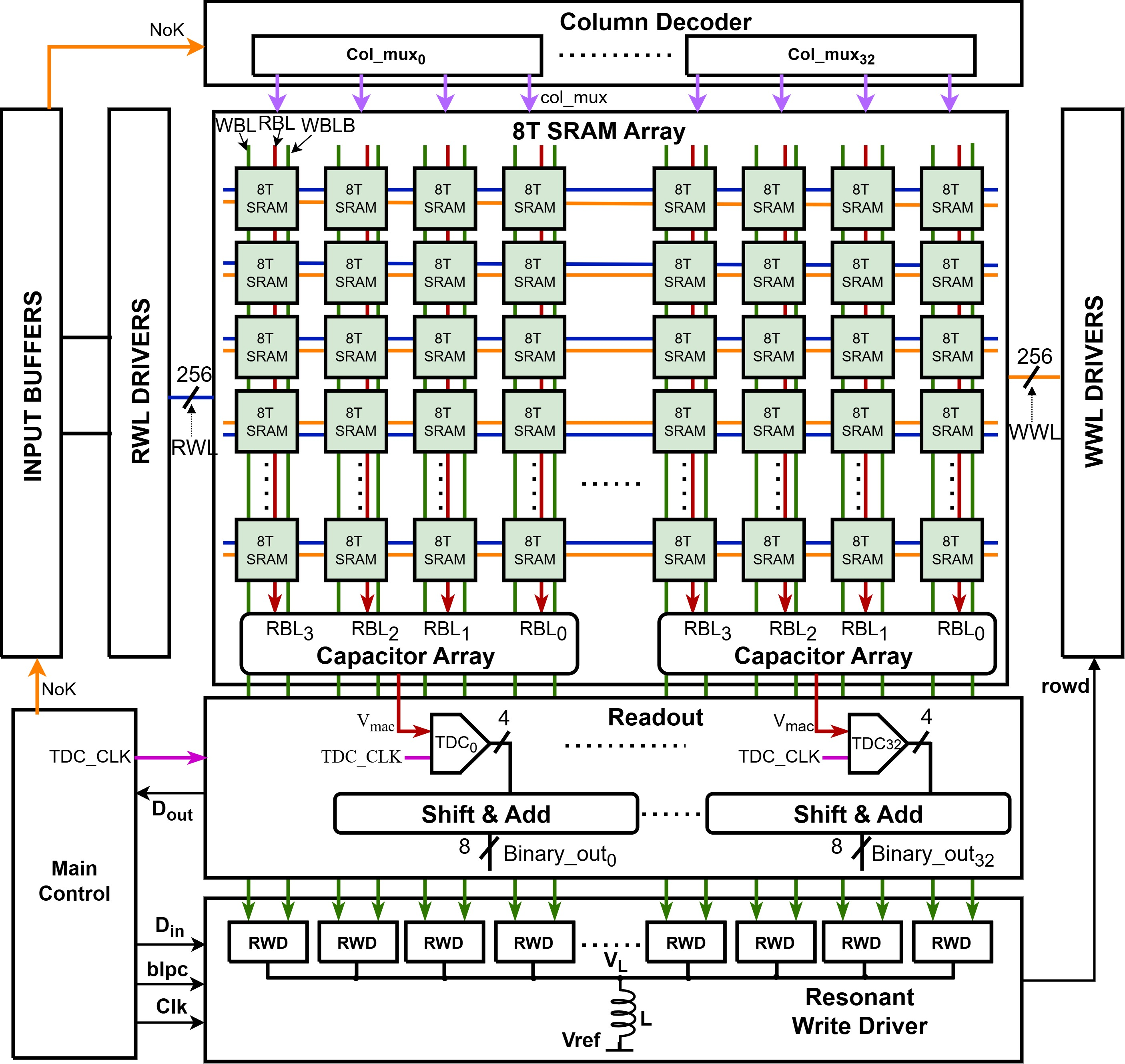
Figure 2: The proposed TDC-CiM macro integrates 8T bitcell array, RWL drivers, TDC readout circuitry, and resonant writeback.
The 8T SRAM bitcell utilizes a decoupled read port (Figure 3a), enabling bitwise multiplication with disturbance-free discharge only when both input and weight are logic '1' (Figure 3b). Multirow activation aggregates multiple bitwise MACs along the bitlines (Figure 3c).
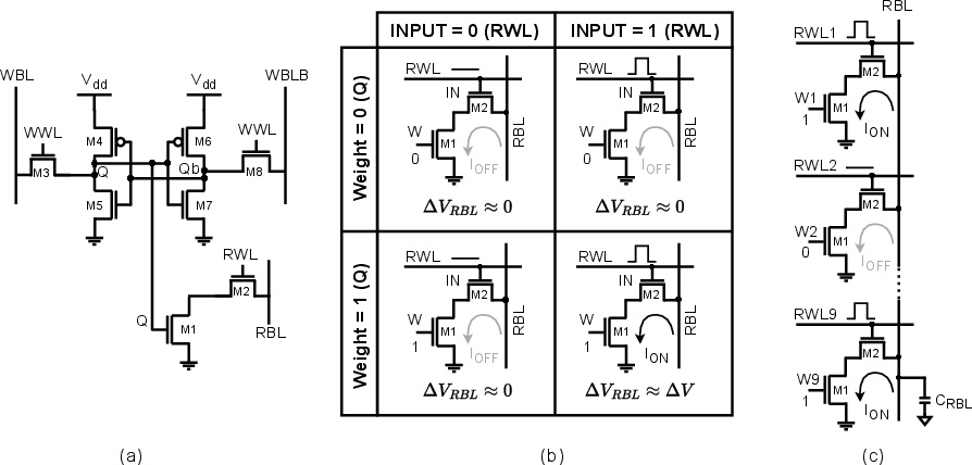
Figure 3: The 8T SRAM array enables robust, parallel, bitwise MAC operations with current-domain accumulation.
Within each MAC operation, input activations are supplied via RWL drivers, and their interaction with stationary weights stored in SRAM cells yields a bitline discharge proportional to the binary multiply-accumulate function (Figure 4). The design uses binary-weighted capacitors for analog accumulation, producing a multi-bit MAC output following controlled charge sharing with the central accumulation capacitor.
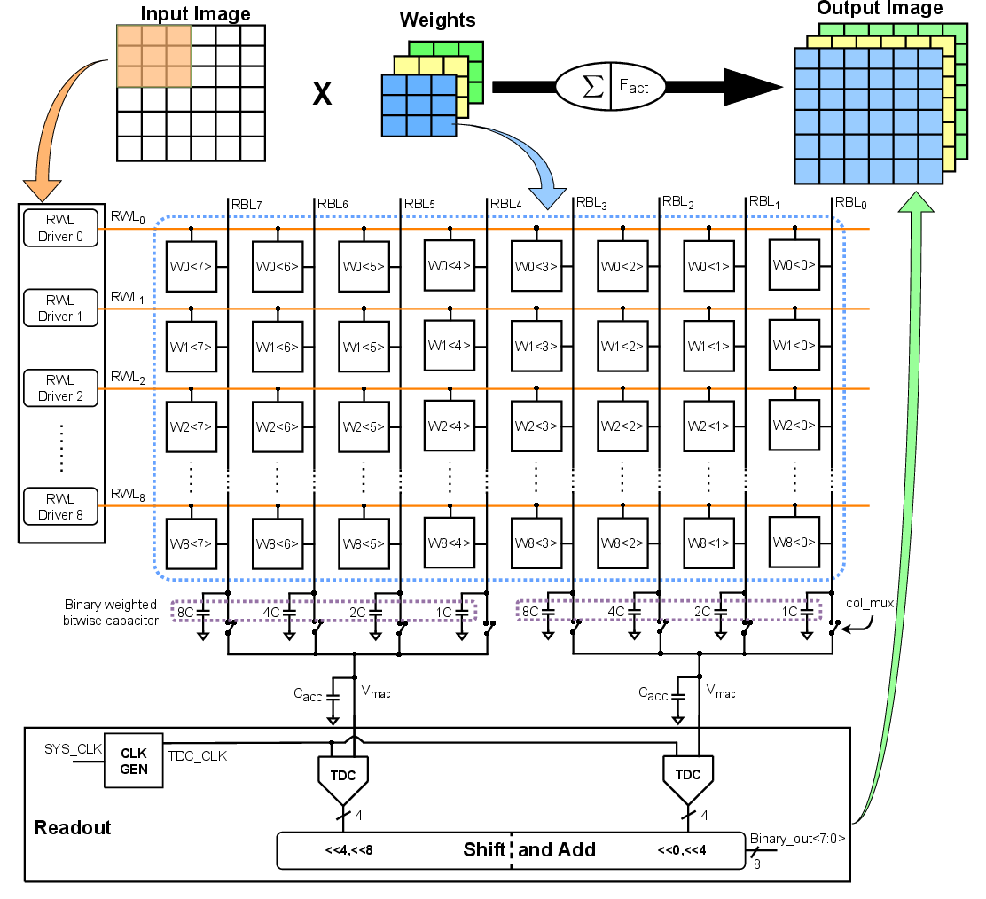
Figure 4: SRAM-executed MAC operation uses input-driven RWLs, stationary weights, and charge-sharing accumulation for analog MAC output.
Figure 5 further shows time-domain simulation of the bitwise MAC on RBLs, resulting in the analog voltage Vmac, subsequently digitized by the TDC.
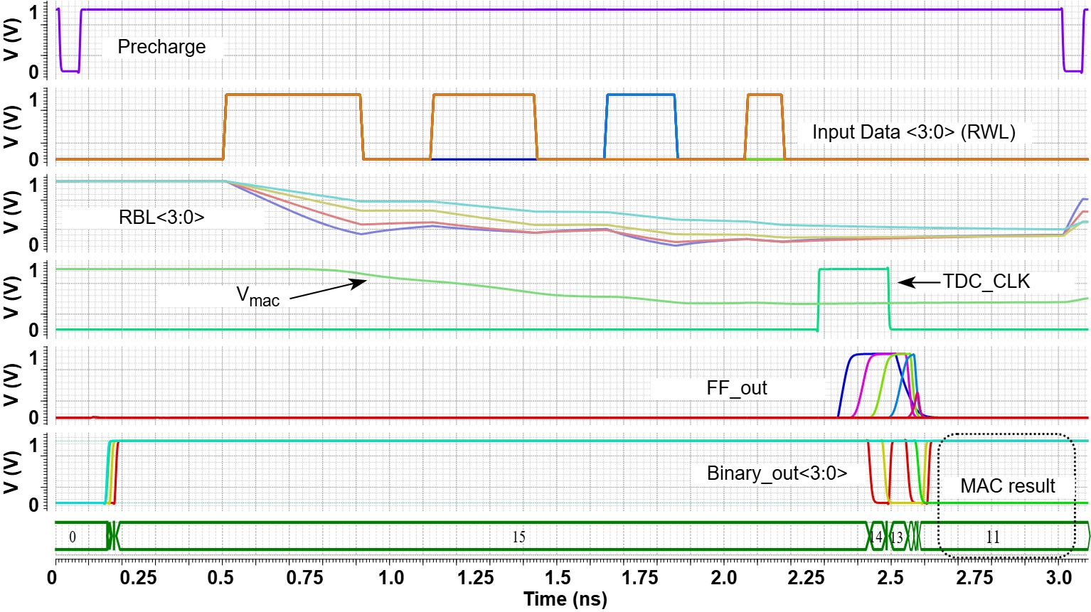
Figure 5: SPICE simulation of bitwise MAC and charge sharing highlights the generation of the analog MAC result.
Time-to-Digital Converter (TDC) Readout
The primary contribution is a custom 4-bit TDC based on pulse-shrinking delay elements and D flip-flops (DFFs). The analog MAC voltage Vmac modulates the delay of the pulse as it propagates through the chain. The pulse count, captured by the DFFs, is then converted by a thermometer-to-binary encoder (Figure 6). The TDC delivers a monotonic, approximately linear digital output as a function of the input analog MAC voltage (Figure 7).
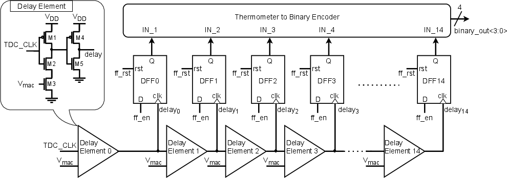
Figure 6: The 4-bit TDC uses pulse-shrinking delay elements and DFFs for digital code generation from analog MAC voltage.
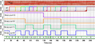
*Figure 7: TDC functionality simulation demonstrates nearly linear digital output with a voltage ramp input
Vmac. *
Unlike conventional TDCs, this design requires no explicit voltage-to-time conversion due to the native time-based MAC readout, resulting in reduced complexity, lower comparator noise sensitivity, and diminished non-linearity. The TDC is tightly co-designed with the MAC’s analog discharge to maximize linearity and dynamic range, as characterized in subsequent DNL/INL analysis (Figures 12–14).
Resonant Energy-Recycling Write Driver
To further minimize energy overhead during memory updates, the architecture employs a resonant write driver (Figure 8). This design uses a shared inductor and four additional transistors to recycle bitline energy, allowing charge recovery during the precharge phase and reducing supply drain.
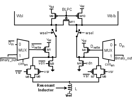
Figure 8: Resonant write driver recycles energy via coordinated inductor switching, supporting high-efficiency writeback.
Figure 9 validates the proper operation of the resonant write driver during bitline updates.
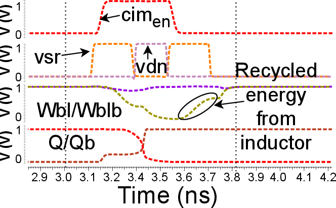
Figure 9: Operation of the resonant write driver during writeback as TDC outputs are stored in SRAM.
Flexible, Weight-Stationary Data Mapping
A fully weight-stationary data mapping algorithm is proposed to optimize SRAM utilization across diverse layers and models. Stationary 8-bit weights are loaded into SRAM banks, while input activations are broadcast via RWL drivers, exploiting local data reuse and alleviating off-chip bandwidth requirements (Figure 10). The method supports flexible parallelism, with automated SRAM macro selection per-model based on kernel dimensions and workload.
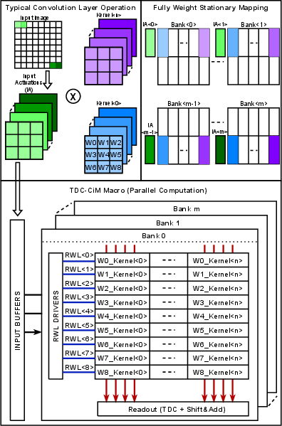
Figure 10: Weight-stationary mapping minimizes off-chip transfers by fixing weights in SRAM and dynamically reusing IFMs.
TDC Precision and Robustness
The TDC’s transfer characteristics follow a nearly monotonic trend, with minor deviation from ideal linearity (Figure 11). DNL values are tightly bounded (±0.4 LSB), and INL deviation does not exceed -1/+0.5 LSB (Figures 13–14), ensuring reliable code distribution without missing codes.
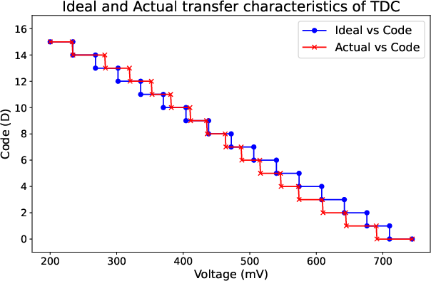
Figure 11: Simulated TDC transfer curve highlights low nonlinearity, critical for consistent MAC digitization.
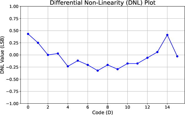
Figure 12: DNL analysis confirms all TDC steps fall within ±0.4 LSB, preventing code loss.
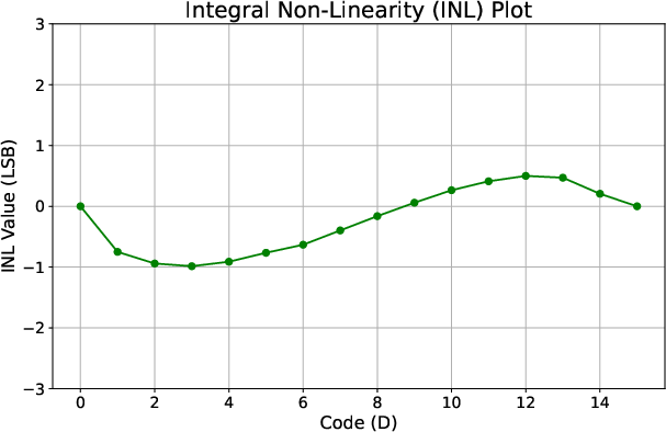
Figure 13: INL deviation remains minimal, demonstrating sufficient linearity for INT8 CNN.
Monte Carlo simulations validate stability under supply voltage (Figure 14) and temperature variation (Figure 15). Delay and power statistics are consistent across VDD (0.9–1.1 V) and temperatures (0–100°C), confirming robust performance under process-voltage-temperature (PVT) variability.
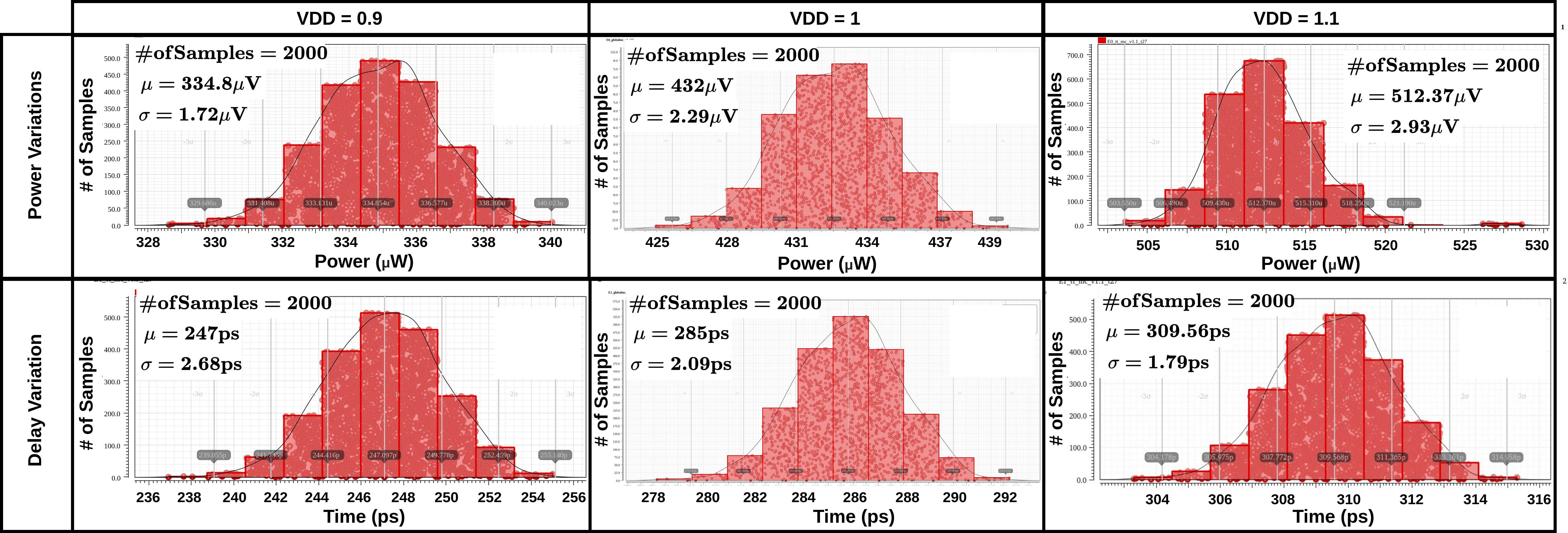
Figure 14: Monte Carlo supply voltage analysis shows robust TDC power and delay behavior across VDD.
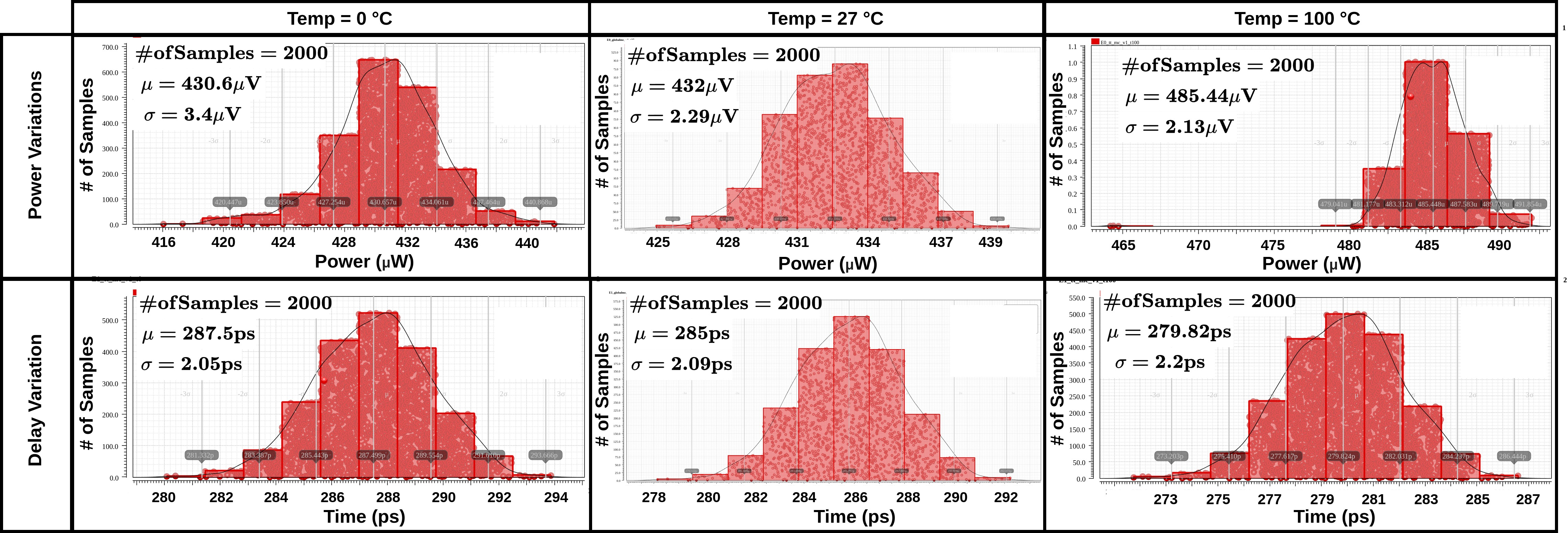
Figure 15: TDC maintains stable operations under temperature variations, as evidenced by power and timing distributions.
Experimental Results and Benchmarks
The architecture is benchmarked using various CNNs—including LeNet-5, MobileNetV1/V2, SqueezeNet, ResNet-18, and Tiny-YOLOv3—quantized to INT8 without fine-tuning. The mapping algorithm determines optimal SRAM sizes for each workload. Figure 16 demonstrates that power consumption remains nearly constant with SRAM scaling, while inference latency and energy consumption sharply decrease with larger SRAM sizes.
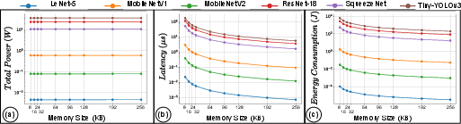
Figure 16: For six CNNs, increasing SRAM size drastically reduces inference latency and energy, with power remaining steady.
Critically, scaling SRAM from 8 KB to 256 KB reduces inference energy by up to 8× (average 67–73.6%) without significant quantization accuracy drop (within 1% across models). Selected SRAM sizes are workload-adaptive (e.g., LeNet-5 requires only 24 KB, while ResNet-18 and Tiny-YOLO demand 256 KB).
The TDC achieves 1 GS/s sampling with just 1.25 mW; post-layout SPICE simulations validate 320 GOPS peak throughput and 38.46 TOPS/W energy efficiency. Compared to prior designs, the approach achieves a 59.7% energy efficiency improvement over [comp_jssc_23], with 6.25× higher throughput than [comp_jssc_24], and power dissipation notably lower than both time-domain and SAR-based ADC designs.
Implications and Future Directions
The TDC-CiM architecture represents a significant reduction in analog-digital conversion bottlenecks for charge-domain SRAM-based CiM. By replacing conventional ADCs with low-power, scalable TDC readouts and augmenting energy recovery through custom write drivers, the system is well-aligned for large-scale, on-chip NN inference under aggressive power and area constraints—necessary for edge AI deployment.
The proposed weight-stationary mapping algorithm and macro selection framework generalize across model depths and network architectures, enabling workload-aware hardware reconfiguration. The design avoids fine-tuning or model retraining for quantization, further streamlining deployment.
Potential future extensions include (1) increasing TDC bit precision to further reduce WALDEN Figure-of-Merit for larger/sensitive models, (2) advanced error compensation via LUT-based code calibration, and (3) architectural integration with hybrid analog-digital CiM macros for transformers or LLM inference. The impact of additional process, voltage, and temperature corners—including ultra-low voltage operation—warrants deeper reliability analysis for emerging memory technologies.
Conclusion
This work introduces a resonant TDC-based CiM architecture using 8T SRAMs for low-power, scalable inference on INT8 CNNs. The design eliminates conventional ADC bottlenecks with a highly efficient TDC readout, realizes robust, low-leakage MACs through architectural innovations in bitcell and write driver design, and supports model-agnostic layer mapping. The result is a platform with competitive throughput and industry-leading energy efficiency, delivering substantial reductions in inference latency and energy consumption for edge-oriented deep learning workloads.