- The paper introduces ONEM, a label-free, non-invasive imaging technique that converts optical near-field patterns into photoelectron emission to achieve 31 nm resolution.
- It integrates single-mode fiber illumination with aberration-corrected LEEM, validated through nanolithography, plasmonic mode imaging, and live-cell studies.
- The method enables real-time, sub-second imaging for dynamic electrochemical and biological processes, paving the way for advanced research in bio- and materials science.
Super-resolution Optical Near-field Electron Microscopy (ONEM) for Bio- and Materials Science
Introduction and Motivation
The paper introduces Optical Near-field Electron Microscopy (ONEM), a super-resolution, label-free, and non-invasive imaging modality that leverages the conversion of optical near-field intensity patterns into photoelectron emission, subsequently imaged via low-energy electron microscopy (LEEM). ONEM circumvents the limitations of conventional optical microscopy, which is fundamentally restricted by the diffraction limit, and electron microscopy, which is often destructive to sensitive samples due to electron-beam-induced damage. By probing samples exclusively with photons and spatially separating the sample from the photoelectrons, ONEM achieves high spatial and temporal resolution while preserving sample integrity, making it particularly suitable for dynamic studies in biology, electrochemistry, and nanophotonics.
ONEM Instrumentation and Resolution
The ONEM setup integrates a single-mode fiber-based optical illumination module with an aberration-corrected LEEM system. The sample is illuminated with visible light (405 nm) at controlled polarization, and the resulting near-field intensities are transduced into a spatially varying electron flux using a thin cesiated graphene or chromium photocathode. The emitted electrons are accelerated and imaged with a lateral resolution of 1.5 nm.
Spatial resolution characterization was performed using a nanolithographically fabricated test sample with alternating chromium and fused silica features. The ONEM image of a 250 nm wide line yielded an upper bound spatial resolution of 31 nm (λ/13), well below the optical diffraction limit.
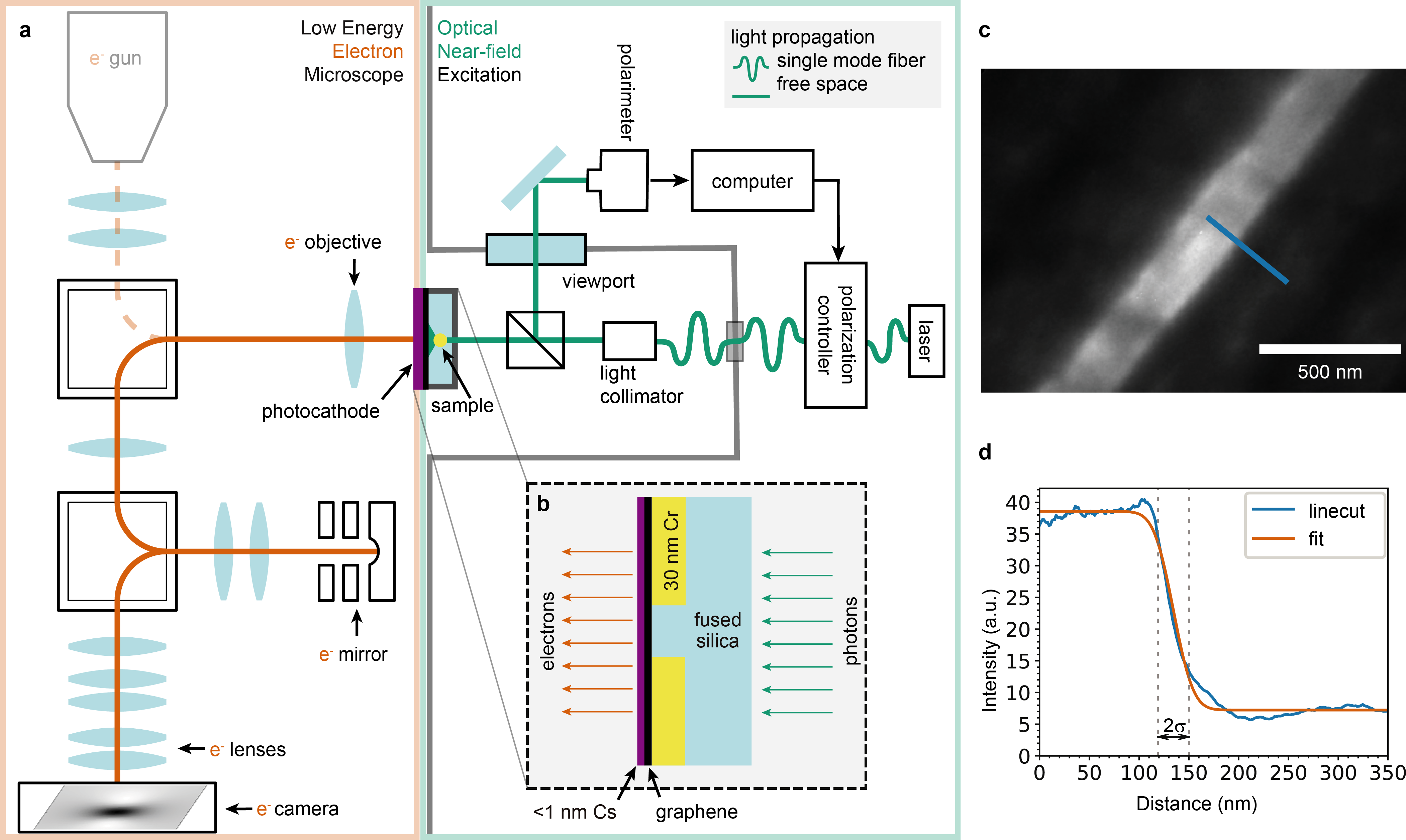
Figure 1: ONEM setup and resolution characterization using a nanolithographic test sample, demonstrating 31 nm spatial resolution.
Plasmonic Imaging Capabilities
ONEM was applied to image localized surface plasmon resonances in 100 nm Ag nanocubes deposited on a silicon nitride window coated with a 3 nm caesiated chromium photocathode. The system enables polarization-resolved imaging, distinguishing between circular and linear polarization responses. The orientation of plasmonic modes can be resolved with exposure times as low as 1 second, and the technique is sensitive to sub-diffraction features that do not propagate to the far field.
Finite-difference time-domain (FDTD) simulations, convolved with a Gaussian matching the experimental resolution, corroborate the observed ONEM images. The method can differentiate between nanoparticle shapes (e.g., nanocubes vs. nanospheres) based on their plasmonic mode signatures.
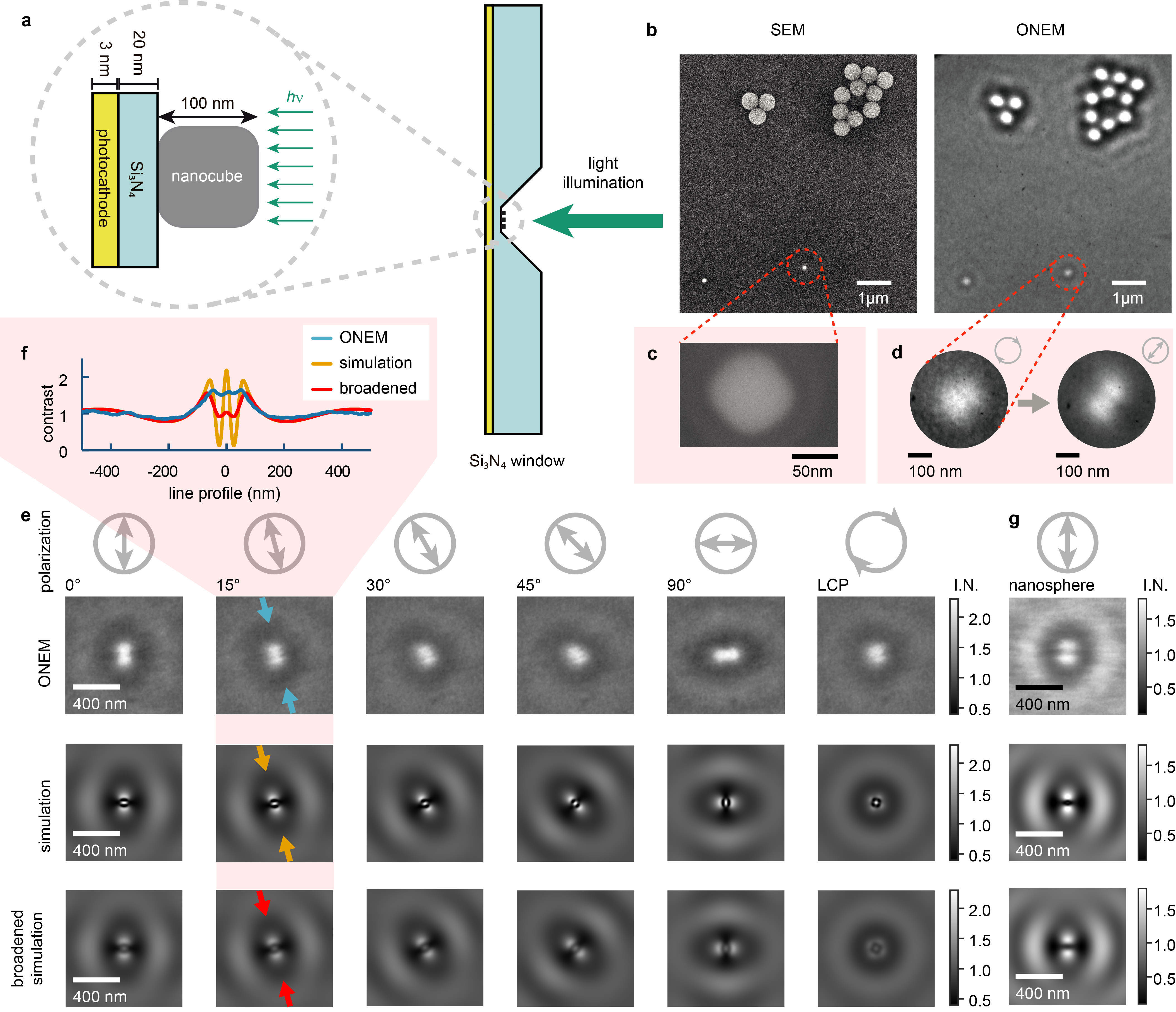
Figure 2: ONEM imaging of Ag nanocube plasmonic modes under varying polarization, with experimental and simulated intensity distributions.
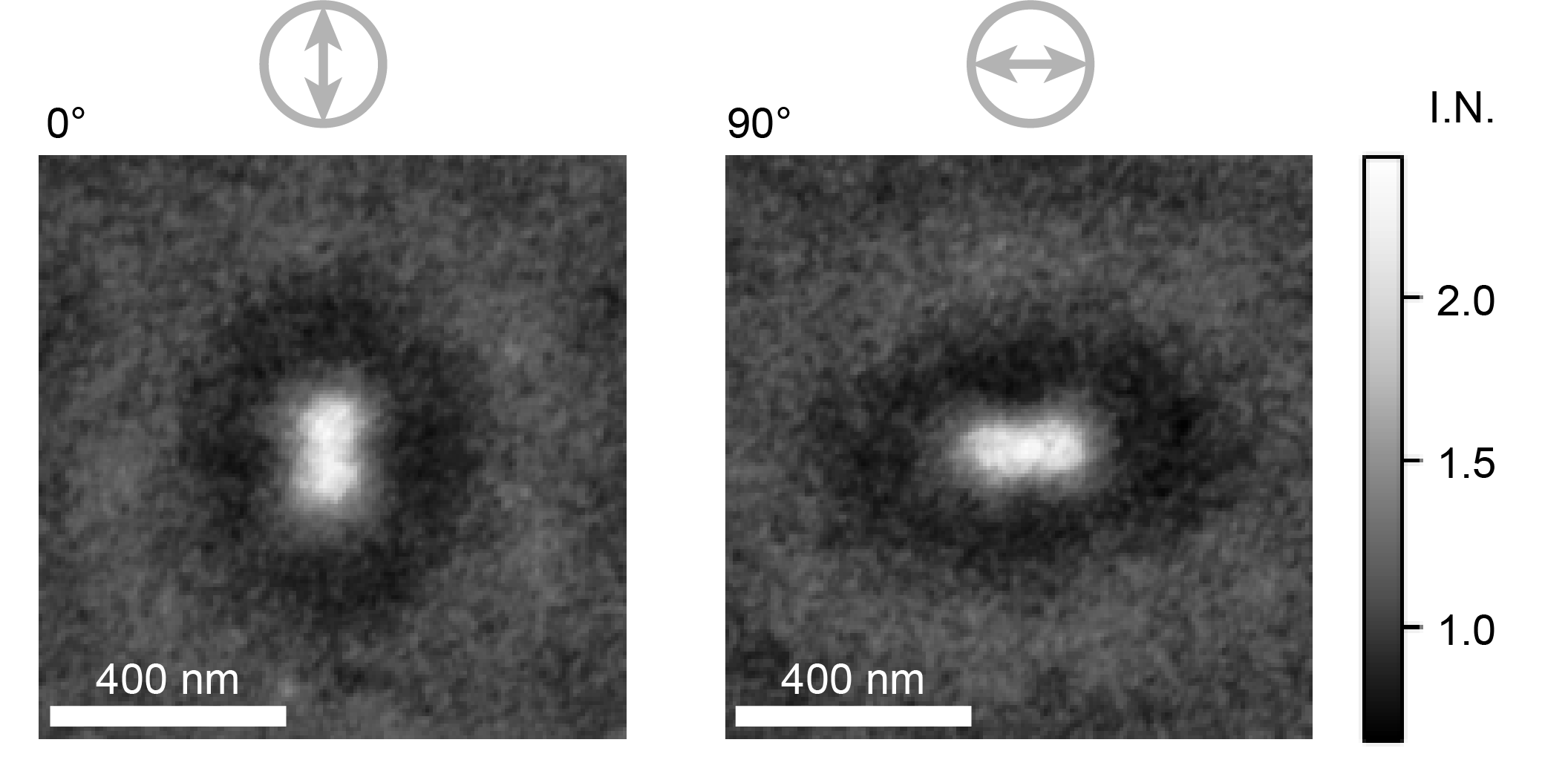
Figure 3: ONEM images demonstrating rapid (1 s) acquisition of plasmon orientation for Ag nanocubes under perpendicular linear polarizations.
Live-cell Imaging in Liquid
A custom-designed ultra-high vacuum-compatible liquid cell was developed for ONEM, enabling imaging of live E. coli bacteria in Lysogeny Broth. The bacteria are confined between a glass window and a silicon nitride chip, separated by an O-ring. ONEM imaging at 3 Hz frame rate over extended periods revealed both mobile and immobile bacteria, with post-imaging optical microscopy confirming cell viability, thus validating the non-invasiveness of the technique.
The ONEM images encode the 3D orientation and distance of the bacteria relative to the photocathode, with simulations (angular spectrum method) providing quantitative agreement. The system is sensitive to morphological changes, such as bending and filamentation, observable in both ONEM and optical microscopy.
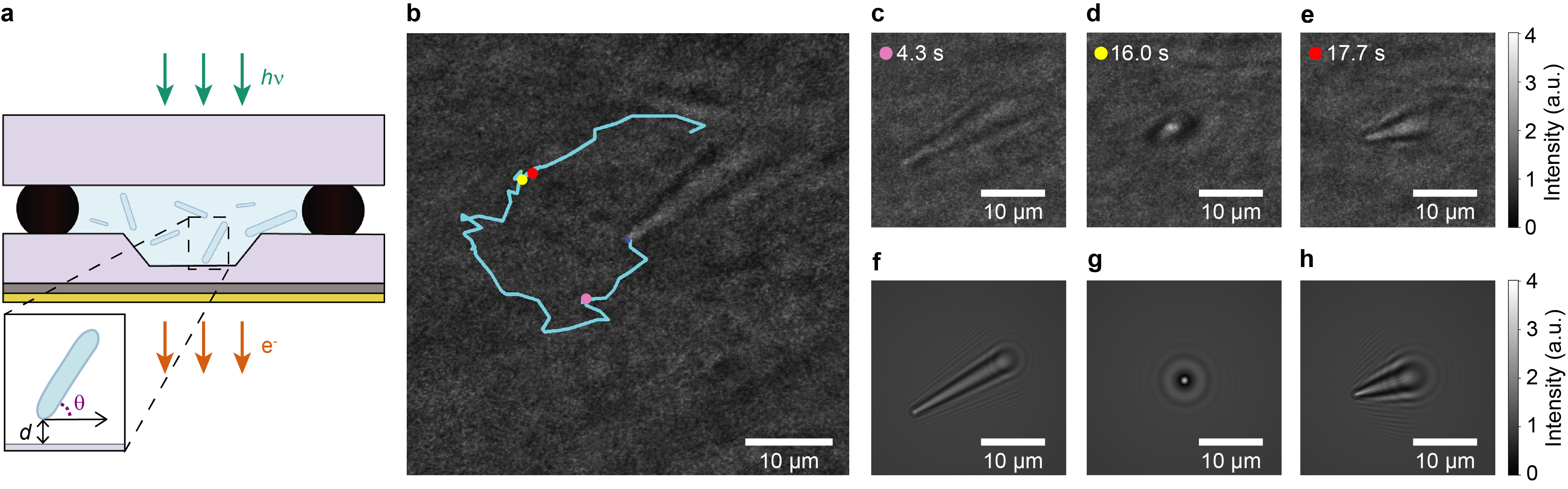
Figure 4: ONEM imaging of live E. coli in liquid, showing bacterial trajectory, selected frames, and corresponding simulations for 3D orientation.
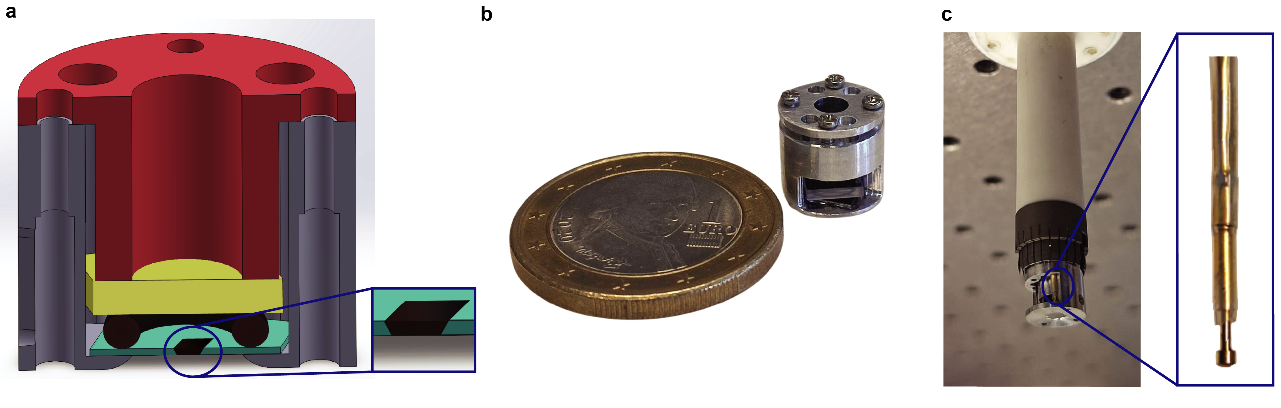
Figure 5: Cross-sectional and assembled views of the ONEM liquid cell, highlighting the design for biological and electrochemical compatibility.
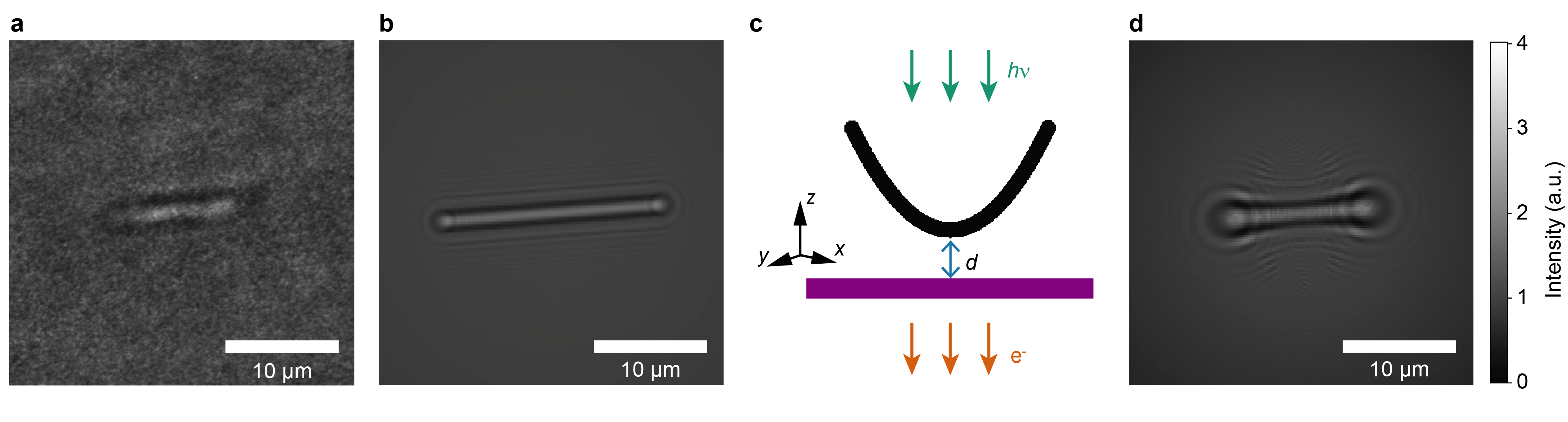
Figure 6: ONEM image and simulation of a bent E. coli bacterium, illustrating sensitivity to dynamic morphological changes.
Real-time Electrochemical Imaging
ONEM was further extended to visualize dynamic electrochemical processes, specifically the nucleation and growth of copper nanoclusters during pulsed electrodeposition on a gold electrode. The liquid cell incorporates two electrodes (working and counter), with copper deposition monitored in real-time via ONEM at 3 Hz frame rate.
The standard deviation of normalized image intensity (σI) serves as a quantitative metric for nucleation and growth dynamics. Post-mortem SEM and EDS analyses confirm copper deposition and morphological evolution, with ONEM providing in situ, real-time insights inaccessible to conventional electron microscopy due to electron-induced artifacts.
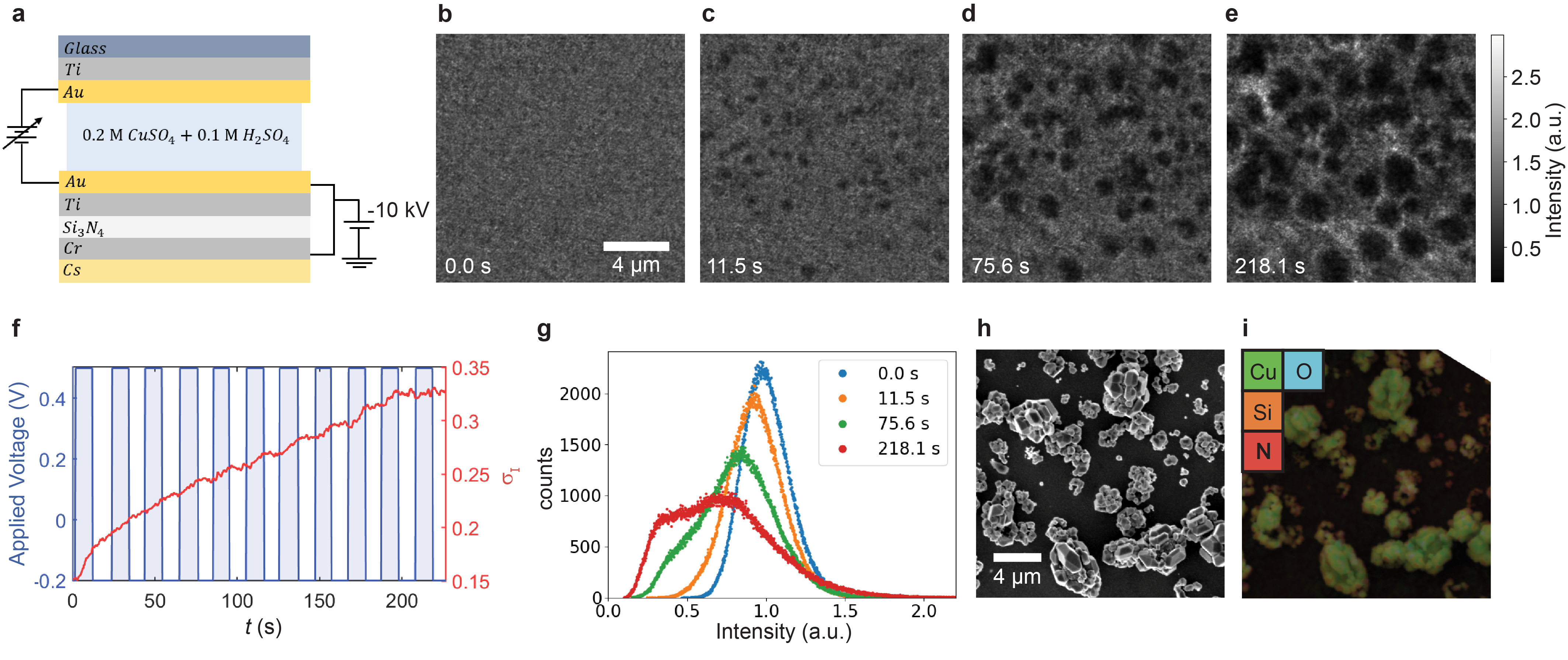
Figure 7: ONEM imaging of pulsed copper electrodeposition, showing temporal evolution, intensity statistics, and post-mortem SEM/EDS confirmation.
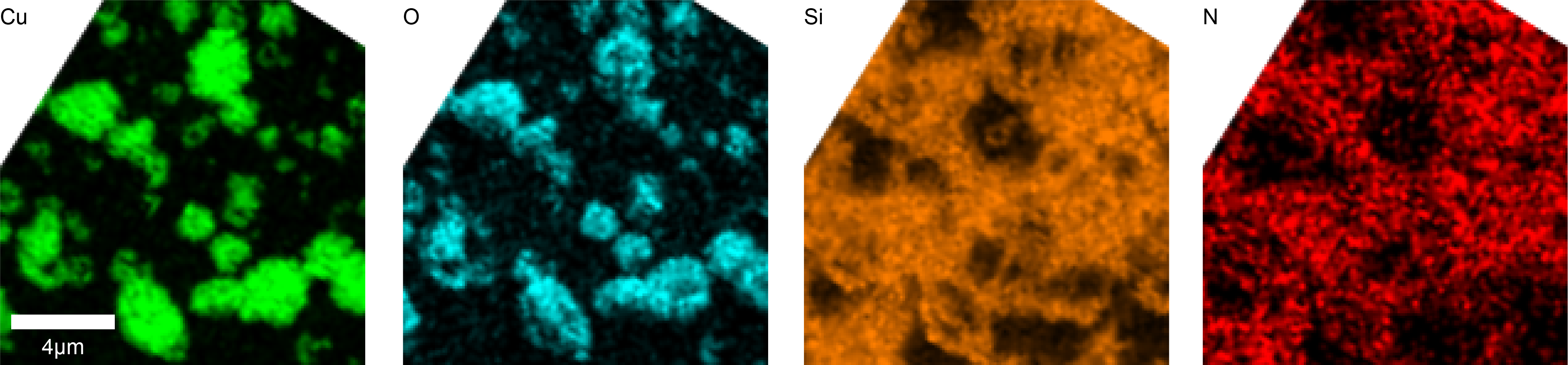
Figure 8: Elemental EDS maps of the electrodeposited region, confirming copper presence and distribution.
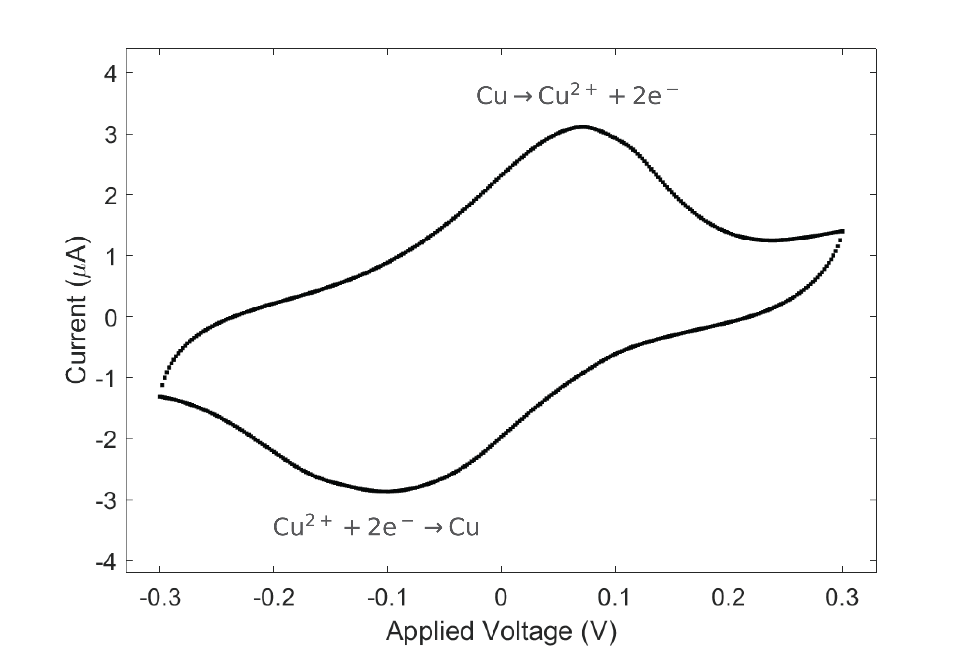
Figure 9: Cyclic voltammetry in the ONEM liquid cell, demonstrating electrochemical control and compatibility.
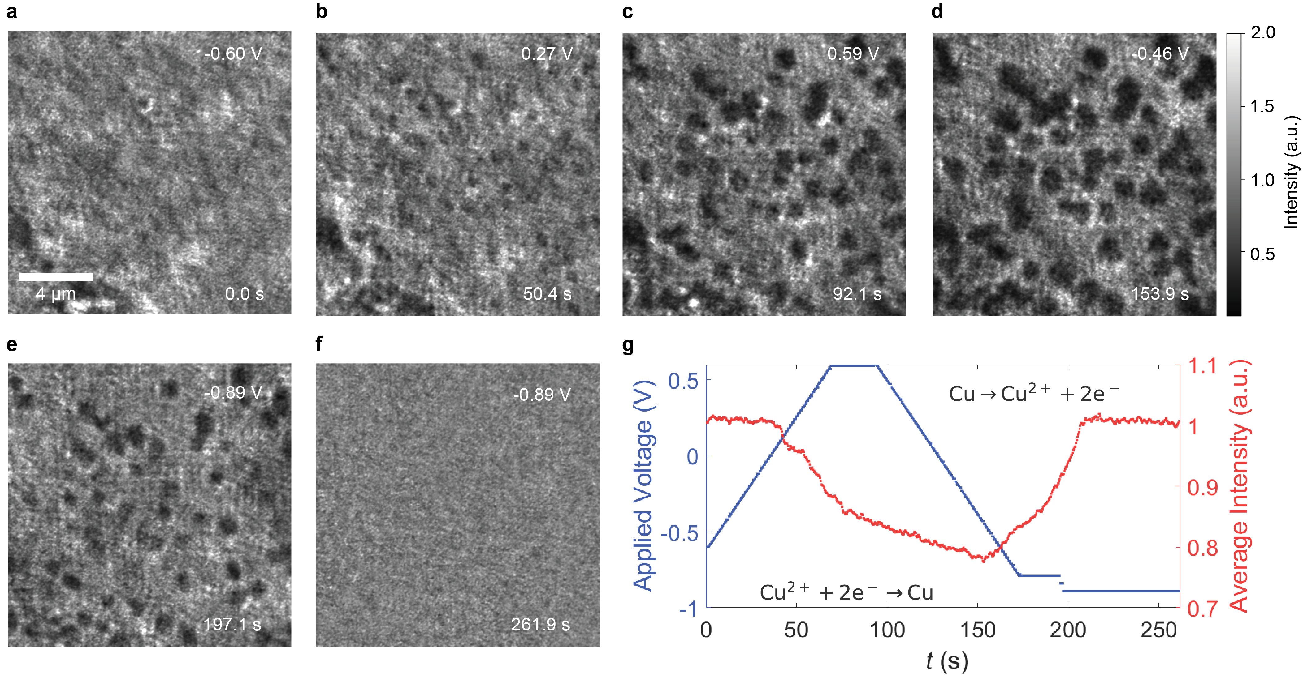
Figure 10: ONEM imaging during cyclic potential sweep, correlating image intensity with copper deposition and stripping.
Technical Implementation and Image Processing
The ONEM optical module utilizes a 405 nm laser diode, single-mode fiber delivery, and a detachable collimator/beamsplitter assembly for polarization control. Photocathode growth is performed in situ via thermal evaporation of Cs onto graphene or chromium supports. Image post-processing includes detector correction, drift correction, Fourier filtering to remove interference artifacts, background normalization, and temporal smoothing.
Simulations for plasmonic and biological samples employ FDTD and angular spectrum methods, respectively, with parameters matched to experimental geometries and refractive indices.
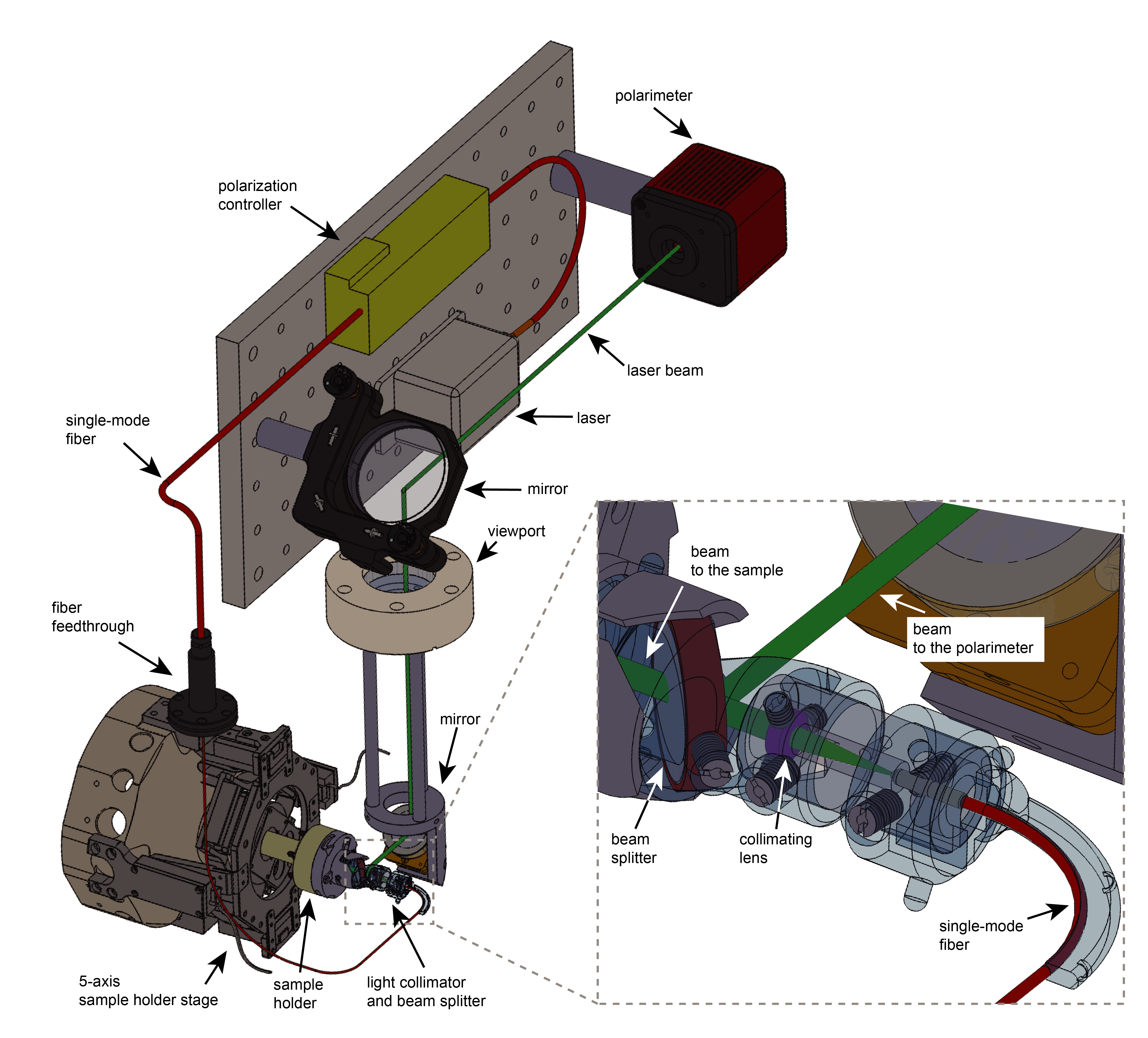
Figure 11: Optical module design for ONEM, detailing fiber delivery, collimation, and polarization control.
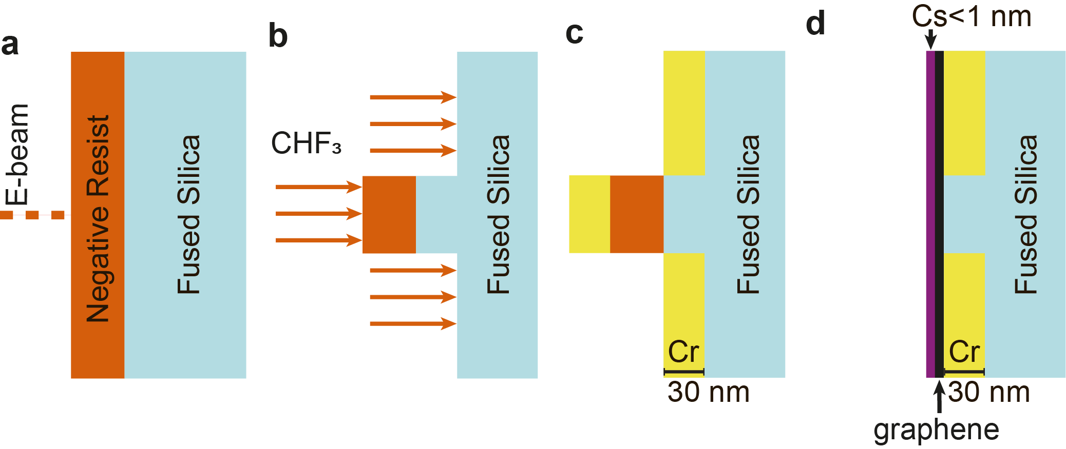
Figure 12: Lithography sample preparation workflow for ONEM resolution characterization.
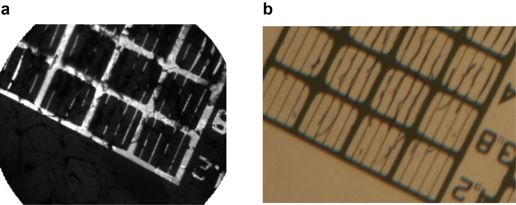
Figure 13: ONEM and optical microscope images of the lithography sample, illustrating sub-diffraction feature resolution.
Implications and Future Directions
ONEM establishes a versatile platform for super-resolution, label-free, and non-invasive imaging across diverse domains. The demonstrated spatial resolution of 31 nm and sub-second temporal resolution enable dynamic studies of light-matter interactions, live-cell behavior, and electrochemical processes without sample perturbation.
Future improvements are anticipated in several areas:
- Resolution and Sensitivity: Thinner support layers (e.g., graphene) and advanced photocathodes with higher quantum efficiency will enhance contrast and reduce invasiveness, particularly for biological applications.
- Detection Efficiency: Low-energy direct electron detectors will improve quantum efficiency and enable shot-noise-limited measurements.
- Electrochemical Quantification: Dedicated three-electrode liquid cells and potentiostat integration will facilitate quantitative electrochemistry.
- Biomolecular Imaging: ONEM's small point-spread function and area electron source are promising for high-throughput applications such as connectomics and molecular dynamics in lipid bilayers.
- Multiplexed Labeling: Site-specificity and multiplexing may be achieved using nanoparticles or antibodies as scattering labels, leveraging their distinct polarizabilities.
The technique's non-invasiveness and high throughput position it as a candidate for real-time in situ studies in catalysis, cellular biology, and nanophotonics, with potential for resolving conformational changes in molecular machines and protein assemblies.
Conclusion
ONEM represents a significant advance in super-resolution microscopy, achieving 31 nm spatial and sub-second temporal resolution in a label-free, non-invasive modality. Its applicability to plasmonics, live-cell imaging, and electrochemistry demonstrates broad utility for dynamic interface studies. The method's technical innovations and future scalability suggest substantial impact on high-throughput, real-time imaging in bio- and materials science.

