- The paper presents the Prinjection technique that injects conductive filament into PCB plated-through holes during a 3D print pause to form strong electrical and mechanical connections.
- It leverages standard ECAD/MCAD workflows with a custom G-code post-processing script to integrate PCB design directly into consumer-grade multi-material FFF printing.
- Experimental results show low contact resistance and improved trace adhesion, enabling reliable fabrication of fully functional, interactive devices.
Printegrated Circuits: Personal Fabrication of 3D Printed Devices with Embedded PCBs
The Printegrated Circuits paper introduces a workflow and technical process for embedding conventional PCBs into 3D printed objects using consumer-grade multi-material FFF printers. The core innovation is the "Prinjection" technique, which injects conductive filament into plated-through holes (PTHs) of PCBs during a mid-print pause, forming robust electrical and mechanical connections between the PCB and the printed structure. This approach addresses the limitations of high-resistance printable conductors and the lack of reliable, scalable interconnects in prior 3D printed electronics, enabling the fabrication of fully functional, interactive devices directly from the printer with minimal post-processing.
Process Overview and Workflow Integration
The Printegrated Circuits process is designed to be compatible with existing digital fabrication workflows, leveraging standard ECAD and MCAD tools, open-source slicers, and unmodified multi-material FFF printers. The workflow consists of:
- ECAD Export: PCB designs are exported as STEP and drill files, providing geometry and PTH locations.
- MCAD Integration: The PCB is imported into a 3D CAD model, and recesses and conductive traces are designed around it.
- Slicing: The model is sliced with material assignments for conductive and non-conductive regions.
- Post-processing: A custom script augments the G-code with pause and Prinjection commands, specifying the PCB insertion layer and PTH locations.
- Printing: The printer pauses for manual PCB insertion, then resumes to perform Prinjection and complete the print.
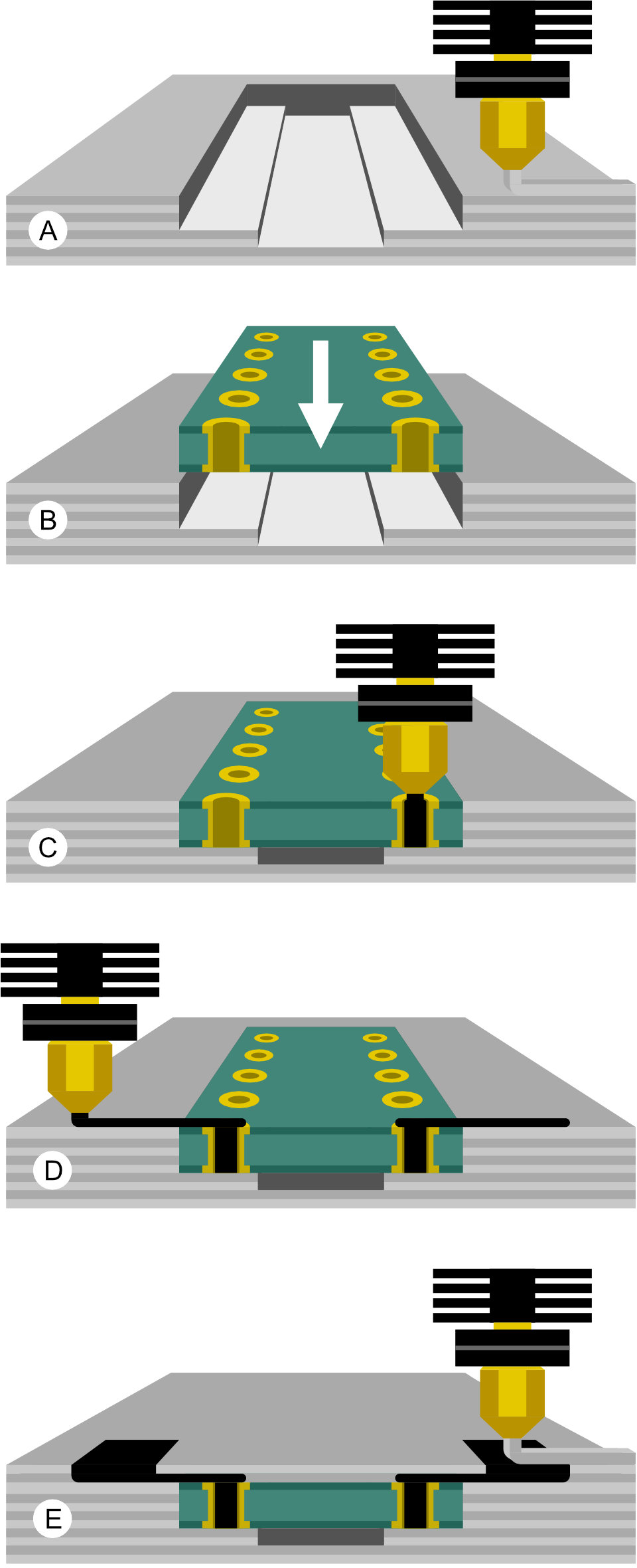
Figure 1: The Printegrated Circuits process, from initial print to PCB insertion, Prinjection, trace printing, and final object completion.
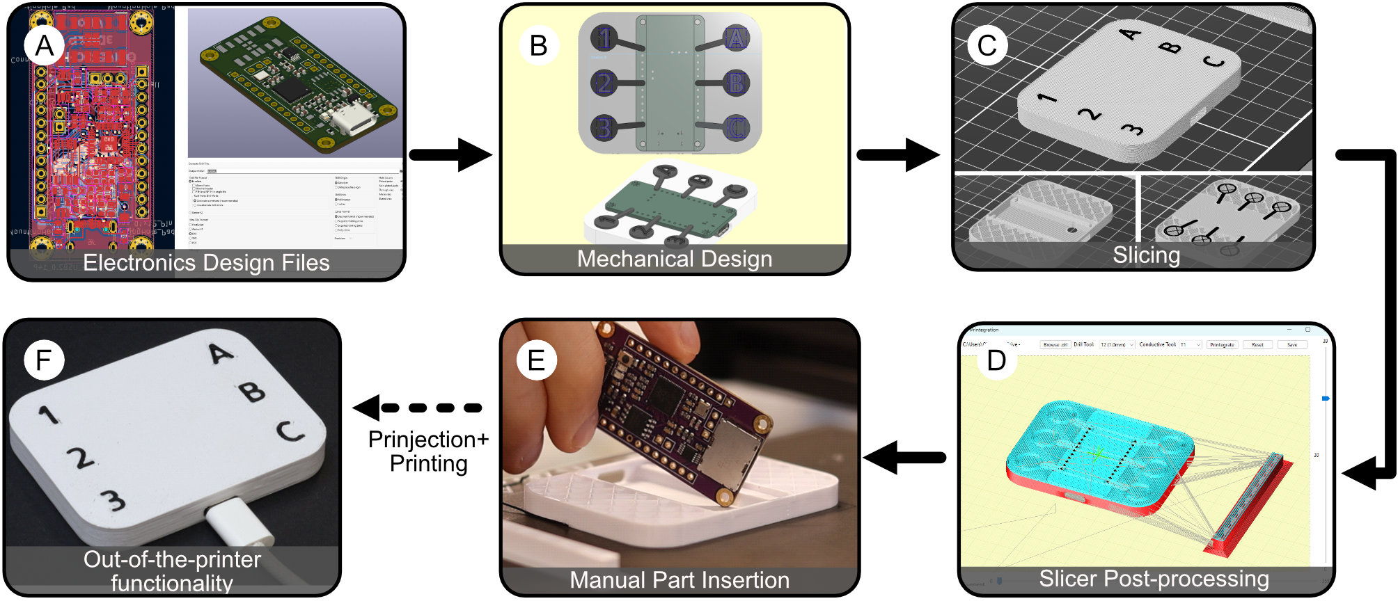
Figure 2: The end-to-end workflow, from ECAD export through MCAD modeling, slicing, post-processing, and printing, culminating in a functional device.
This workflow is accessible to practitioners familiar with standard 3D printing and PCB design, requiring only the addition of the post-processing script and minor design constraints (e.g., PCB orientation, recess design).
Prinjection: Technical Details and Optimization
Prinjection is the central technical contribution, enabling reliable electrical and mechanical connections between the 3D print and the embedded PCB. The process involves:
- Moving the print head to each PTH location.
- Lowering the nozzle to the PCB surface.
- Extruding a calibrated volume of conductive filament into the hole.
- Wiping the nozzle to minimize stringing.
- Lifting and moving to the next hole.
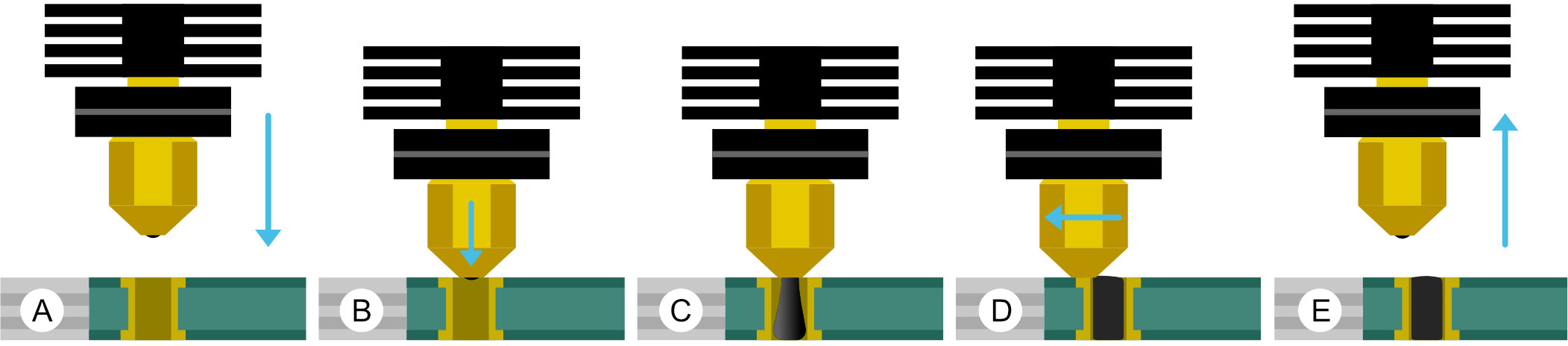
Figure 3: Stepwise illustration of Prinjection movements: approach, lower, inject, wipe, and lift.
Cross-sectional analysis demonstrates that Prinjection fills the PTH with conductive material, maximizing contact area with the plated barrel and providing a mechanical anchor for subsequent trace layers.
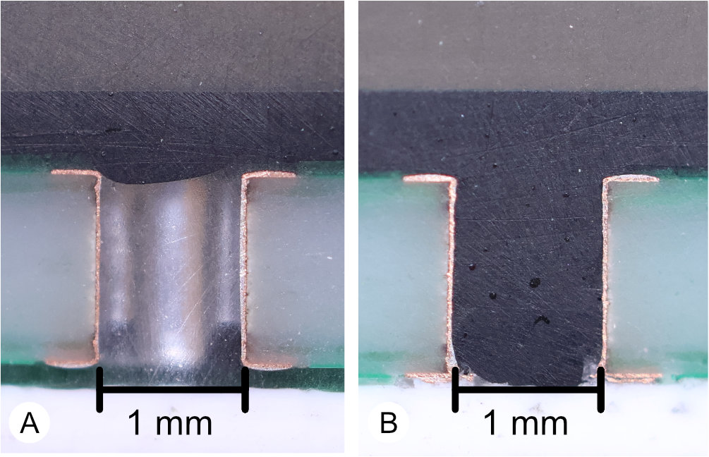
Figure 4: Cross-sections of PTHs: (A) surface-printed trace with poor contact; (B) Prinjected hole fully filled, ensuring robust connectivity.
Parameter optimization experiments determined that an extrusion length of 0.65 mm, retraction of 7.5 mm, and a 2 mm wipe length yield the best results for 1 mm diameter, 1.6 mm thick PTHs, balancing fill quality and stringing.
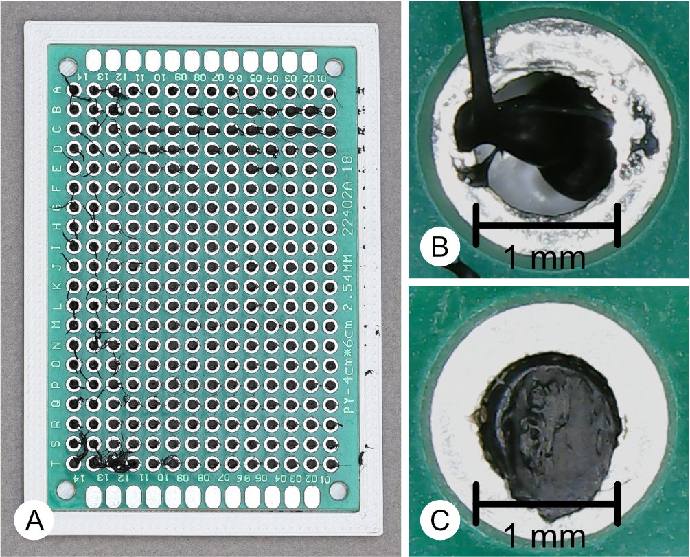
Figure 5: Prinjection optimization: (A) grid of test holes; (B) under-filled; (C) optimally filled hole.
Electrical and Mechanical Characterization
Contact resistance and mechanical robustness were rigorously evaluated:
- Contact Resistance: Four-point probe measurements on custom PCBs showed that Prinjected contacts have resistance on the same order as the bulk trace, with low variance and a 0% failure rate, compared to high and variable resistance and a 10% failure rate for planar-printed contacts.
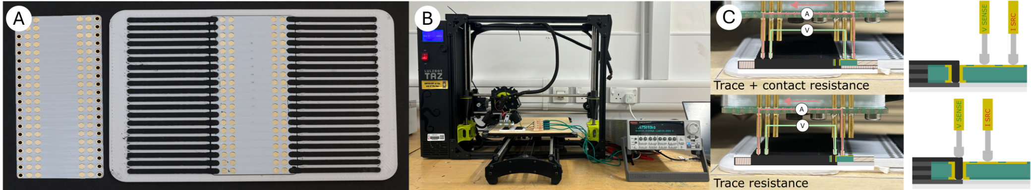
Figure 6: Automated contact resistance measurement setup using a 4-point probe and custom PCB.
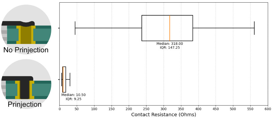
Figure 7: Box plots showing significantly lower and more consistent contact resistance for Prinjected vs. planar contacts.
- Mechanical Robustness: Three-point bend tests (100 cycles at 75 N) revealed that Prinjected contacts not only maintained connectivity but often improved in resistance post-stress, while planar contacts degraded or failed.
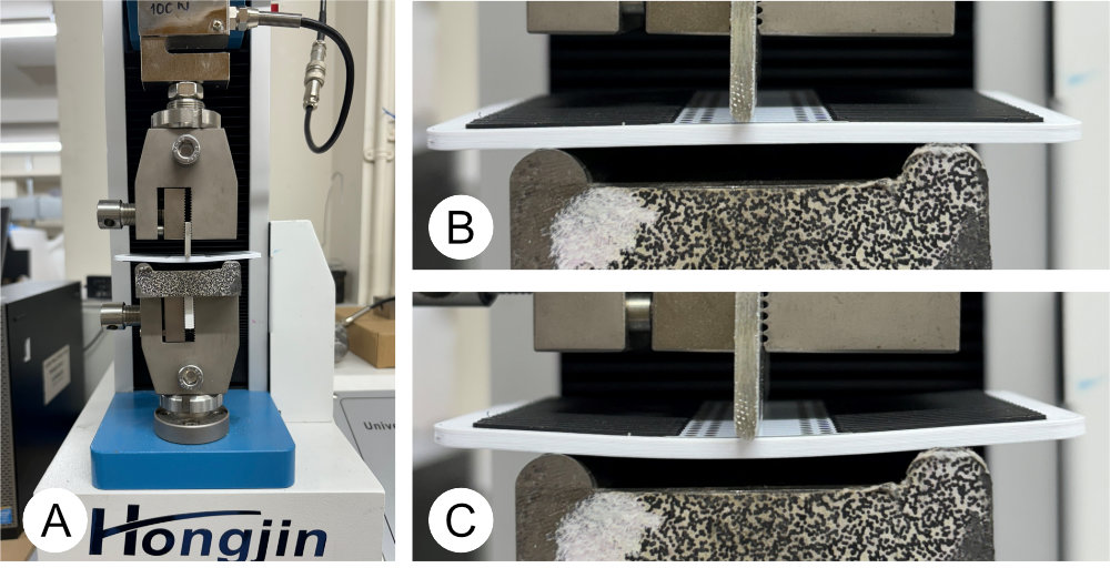
Figure 8: Universal testing machine setup for mechanical robustness evaluation.
- Trace Anchoring: Prinjection prevents delamination of conductive traces from the PCB surface, a common failure mode in planar-printed approaches.
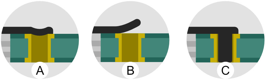
Figure 9: Comparison of trace adhesion: (A,B) planar traces peel; (C) Prinjected traces remain anchored.
Demonstrations and Application Space
Six demonstration devices illustrate the versatility and practical utility of Printegrated Circuits:
- Customizable HID Devices: The "slug," "ladybird," and "isopod" are USB HID devices with unique forms and functions, all using the same Printegrated Circuit Board for capacitive touch and haptic feedback.
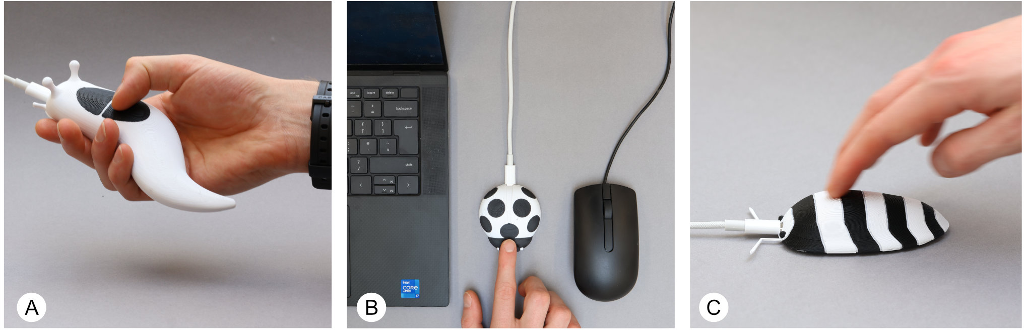
Figure 10: Three distinct HID devices (slug, ladybird, isopod) sharing a common PCB and workflow.
- Iterative Design: The "TuneShroom" MIDI instrument demonstrates rapid iteration of complex 3D routing and touch pad design, leveraging parametric CAD and local fabrication.
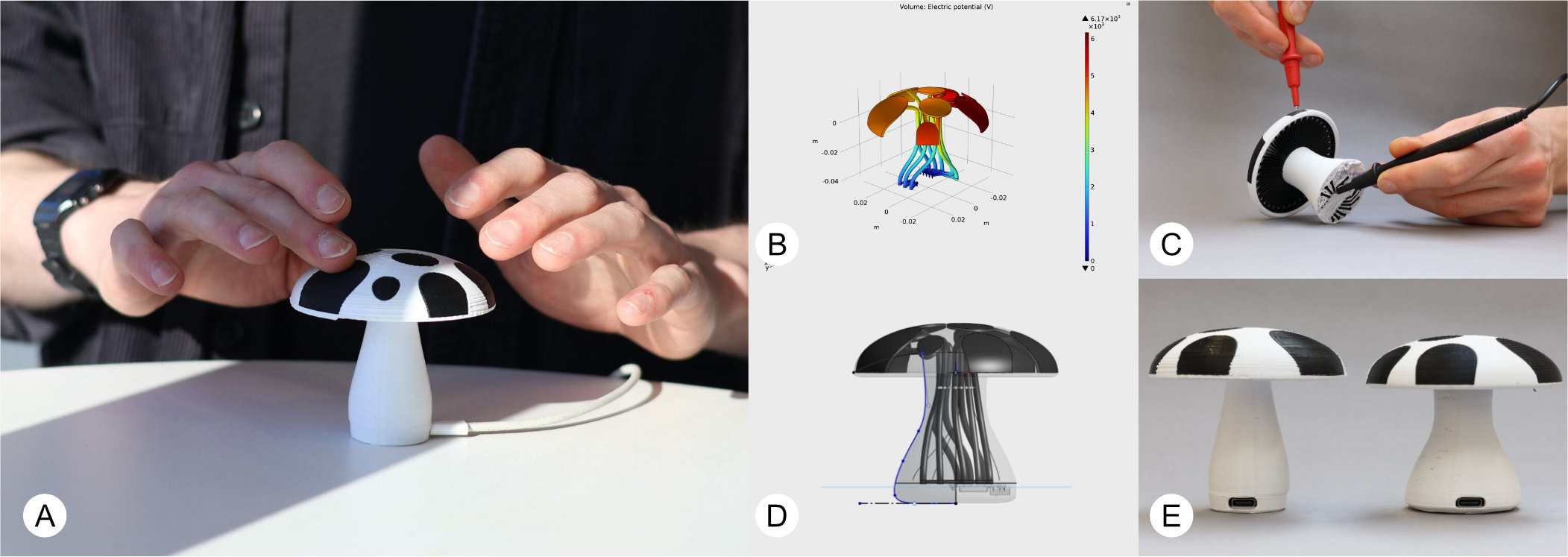
Figure 11: The TuneShroom MIDI instrument, highlighting rapid iteration and simulation-to-fabrication workflow.
- Sensor Integration: "SnailSense" is a plant pot moisture sensor using resistive soil sensing, with iterative electrode design and integration.
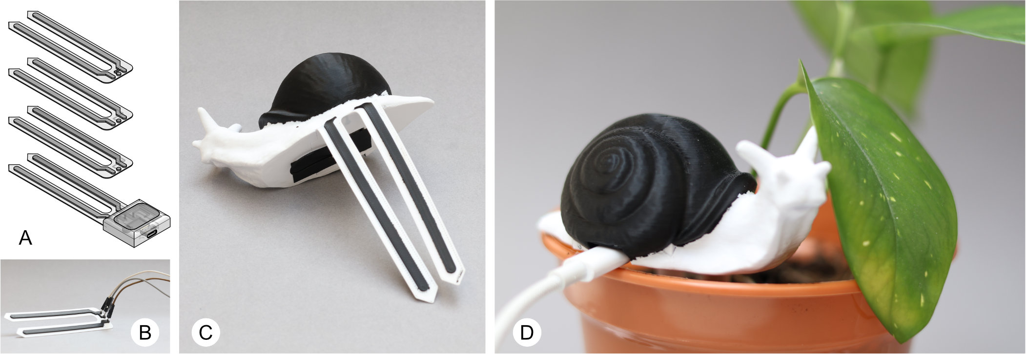
Figure 12: SnailSense moisture sensor, showing iterative electrode prototyping and final Printegrated device.
- Modular Data Physicalization: The "Lego Data Physicaliser" uses resistive towers to record tangible data, demonstrating scalable, modular device fabrication.

Figure 13: Data Physicalisation Device using resistive Lego-style towers for tangible data entry.
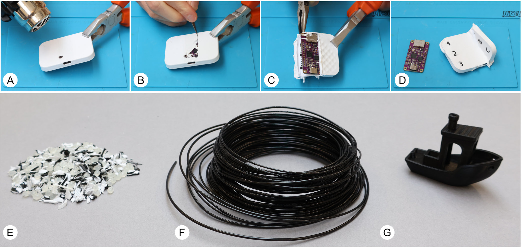
Recovery, Recycling, and Sustainability
The process supports recovery of valuable PCBs and partial recycling of printed materials:
Implications, Limitations, and Future Directions
Practical Implications
- Robust, Out-of-the-Printer Devices: Printegrated Circuits enable the direct fabrication of fully functional, robust interactive devices without post-print wiring or assembly.
- Workflow Compatibility: The process integrates with existing ECAD/MCAD/CAM toolchains and consumer hardware, lowering adoption barriers.
- Scalability: The approach supports small-batch production and rapid iteration, addressing the gap between prototyping and deployable devices.
Theoretical Implications
- Hybrid Fabrication Paradigm: By treating PCBs as reusable "material" and leveraging digital fabrication for form and interconnects, Printegrated Circuits bridge component-centric and material-centric approaches.
- Parameterizable, Predictable Interconnects: The low-variance, robust electrical properties of Prinjected contacts enable reliable modeling and simulation of device behavior.
Limitations
- Material Constraints: The approach is limited by the resistivity of available conductive filaments, restricting high-current applications to the PCB domain.
- Manual Intervention: Mid-print PCB insertion remains a manual step, though it is compatible with intermittent interaction paradigms in digital fabrication.
- Design Complexity: While the workflow is accessible, complex 3D routing of traces and optimal PCB placement may require advanced CAD skills.
Future Directions
- Automated Routing and Toolchain Integration: Incorporating automated 3D trace routing and deeper integration with ECAD/MCAD tools would further lower the barrier for non-experts.
- Advanced Materials: Adoption of lower-resistance filaments or post-print metallization (e.g., electroplating) could expand the range of applications.
- Embedded Output Modalities: Integration of displays, actuators, and energy storage within the Printegrated workflow is a promising avenue.
- Sustainability: Improved recycling methods for multi-material prints and exploration of biodegradable or bio-derived conductive materials could enhance environmental impact.
Conclusion
Printegrated Circuits represent a significant advance in the personal fabrication of interactive devices, enabling robust, fully integrated electronics within 3D printed forms using accessible tools and materials. The Prinjection technique overcomes longstanding challenges in 3D printed interconnects, providing low-resistance, mechanically stable, and repeatable connections between conventional PCBs and printed structures. The demonstrated workflow supports rapid iteration, customization, and small-batch production, with strong implications for HCI, prototyping, and the democratization of hardware development. Future work should focus on expanding material capabilities, automating design steps, and further integrating sustainability into the fabrication lifecycle.