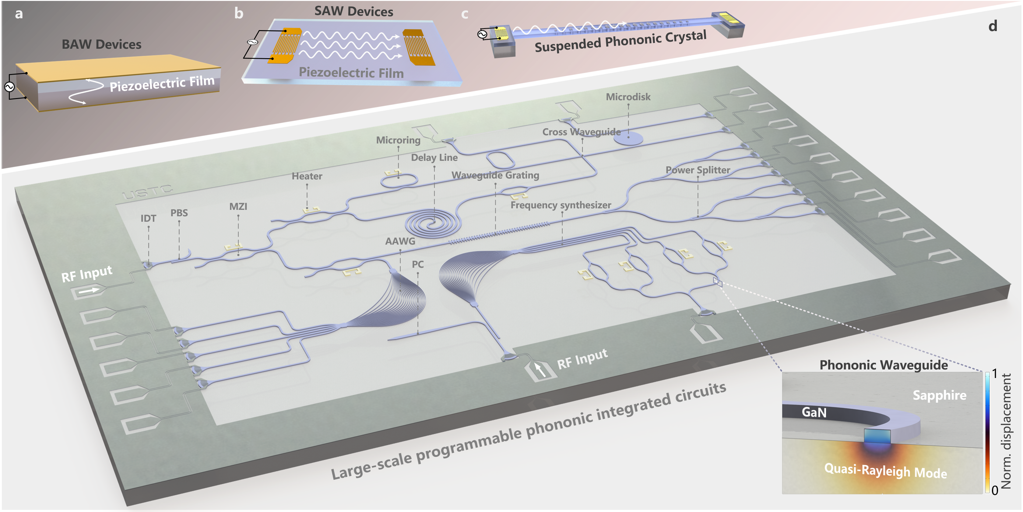
Large-scale programmable phononic integrated circuits (2510.26596v1)
Abstract: Electronic and photonic chips revolutionized information technology through massive integration of functional elements, yet phonons as fundamental information carriers in solids remain underestimated. Here, we demonstrate large-scale programmable phononic integrated circuits (PnICs) for complex signal processing. We developed a comprehensive library of gigahertz-frequency phononic building blocks that control acoustic wave propagation, polarization, and dispersion. Combining these elements, we demonstrate an ultra-compact 1$\times$128 on-chip acoustic power splitter with unprecedented integration density of 3,000/cm$2$, a 21-port acoustic frequency demultiplexer with 3.8~MHz resolution, and a four-channel reconfigurable frequency synthesizer. This work establishes scalable phononic integration as the third pillar of information processing alongside electronics and photonics, enabling hybrid chips that combine all three domains for advanced signal processing and quantum information applications.
Paper Prompts
Sign up for free to create and run prompts on this paper using GPT-5.
Top Community Prompts
Explain it Like I'm 14
Overview
This paper is about making “sound chips” that can handle information, like how electronic chips use electricity and photonic chips use light. The authors build large, programmable phononic integrated circuits (PnICs), which guide and control tiny sound waves inside a solid material. Their goal is to show that sound can be used on chips for complex tasks such as splitting signals, sorting different frequencies, and generating new signals—at scales similar to today’s electronic and photonic circuits.
What questions did the researchers ask?
- Can we build many small, reliable parts that control sound on a chip, the way we do for electronics and photonics?
- Can we connect these parts to make large, complex sound-processing systems?
- Can these systems split one sound into many paths, sort sound by frequency, and flexibly create new signals?
How did they do it?
The team made their chips on a solid platform (no fragile suspended parts), using gallium nitride on sapphire—materials that guide sound waves much like glass guides light in fiber optics. Inside the chip, sound travels through narrow “waveguides,” which you can imagine like tiny pipes for sound.
They designed and tested a toolkit of basic parts, then combined them into bigger systems. Here are the key building blocks, explained with simple analogies:
Key parts (building blocks)
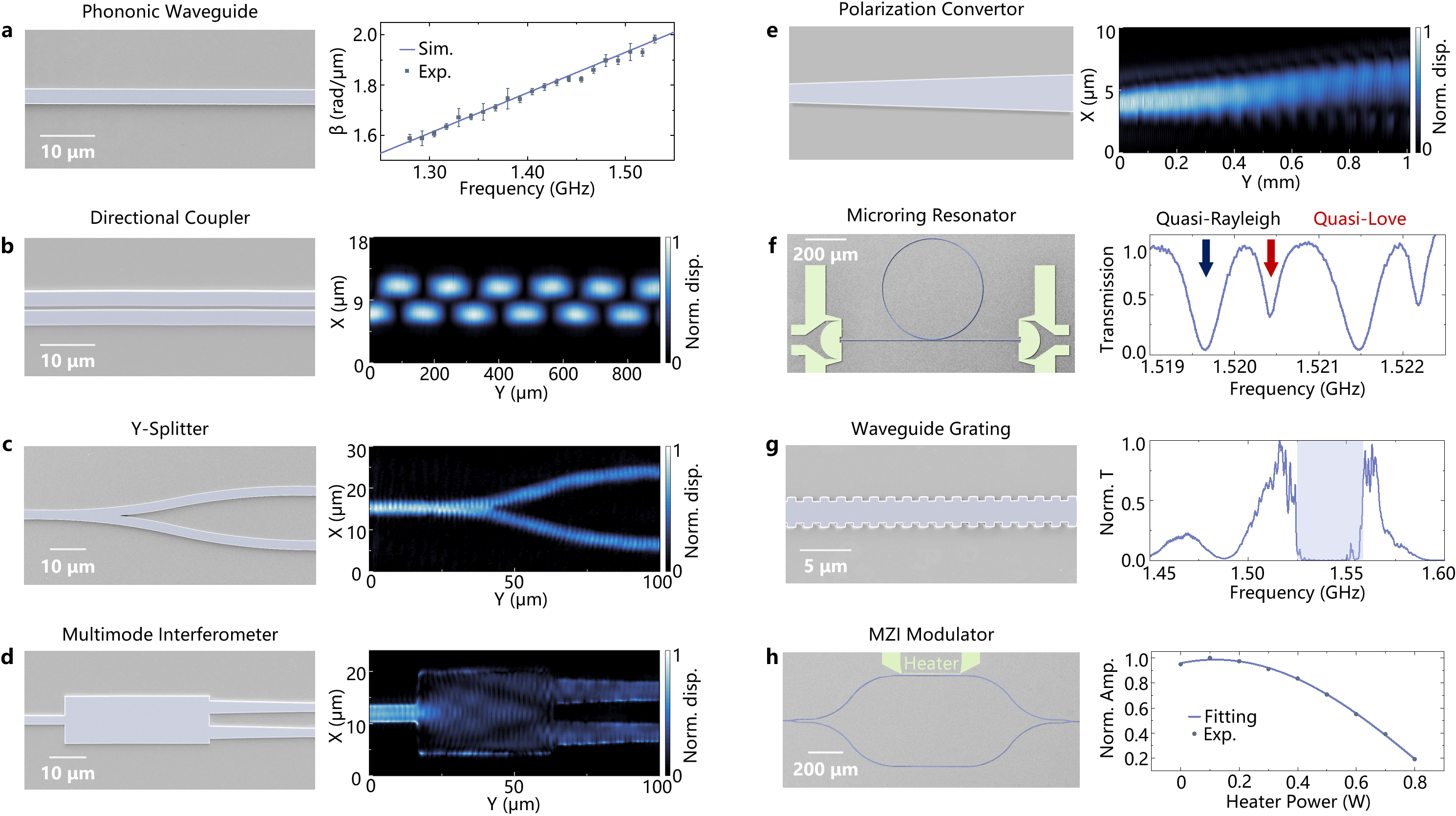
- Directional coupler: Two “sound pipes” placed side by side so sound can hop between them. Like two nearby lanes where cars can switch back and forth depending on the road length.
- Y‑splitter: A single “pipe” that forks into two equal paths. Think of a river splitting into two streams, each getting half the water.
- Multimode interferometer: A wider “room” where different wave patterns mix and split in controlled ways. Like clapping in a hall and using echoes to send sound to different exits.
- Polarization converter: Sound can shake the surface mostly up‑and‑down (Rayleigh) or side‑to‑side (Love). This part gently changes one kind into the other by slowly shaping the “pipe,” like twisting a rope so the kind of wave on it changes.
- Microring resonator: A circular “race track” where only certain sound frequencies fit perfectly and go round and round. It can also separate the two types of waves (up‑down vs side‑to‑side).
- Waveguide grating: A pipe with a repeating pattern that blocks a narrow band of frequencies, like a fence that stops people of a certain height from passing.
- Mach–Zehnder interferometer (MZI) with heater: Splits sound into two paths, then recombines them. Small heaters change the timing of one path, so the waves either add up (loud) or cancel (quiet). Like two friends singing—if one speeds up or slows down, their voices can harmonize or clash.
They used microscopes and vibration sensors to “see” where the sound was going and measure how strong it was at different places and frequencies.
What did they find?
The team combined the building blocks to make three major systems:
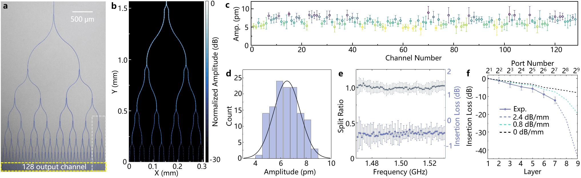
- A 1×128 power splitter:
- One input sound wave is split evenly into 128 outputs using a tree of Y‑splitters.
- It’s extremely compact, with about 3,000 splitters per square centimeter.
- The outputs are very uniform, showing the parts are consistent and the chip is well‑made.
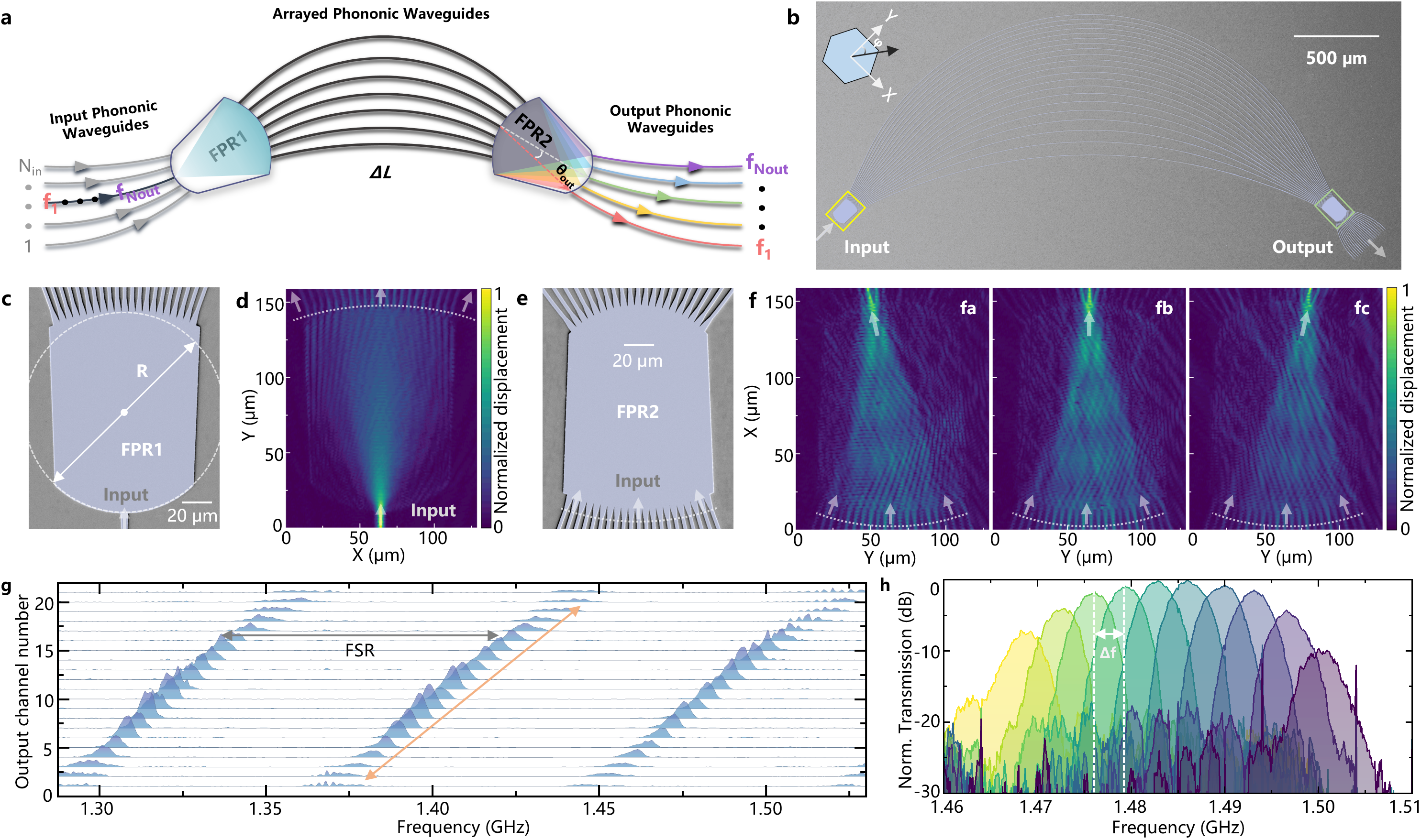
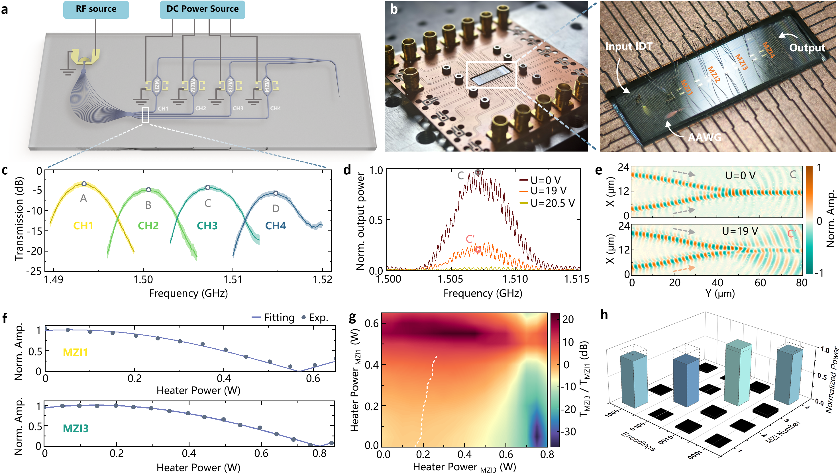
- A 21‑port acoustic arrayed waveguide grating (AAWG) for frequency sorting:
- This is like a “sound prism” that sends different sound frequencies to different output ports.
- It separates frequencies with a fine resolution of about 3.8 MHz and repeats its pattern every ~81 MHz (the free spectral range).
- It cleanly isolates neighboring channels by more than 10 dB (and about 20 dB for the next ones), meaning little “leakage” between them.
- A reconfigurable acoustic frequency synthesizer:
- They used the AAWG to split an input signal into four frequency channels.
- Each channel passes through an MZI with a heater, so they can turn channels on/off or adjust their strength.
- Finally, the channels are combined, letting the chip create or shape signals on demand.
- They demonstrated strong on/off control for each channel, showing the system is programmable.
Why it matters
- Third pillar of information processing: Electronics (electricity) and photonics (light) already power our devices and the internet. This work shows phononics (sound in solids) can join them as a serious, scalable platform.
- Compact and efficient: Sound waves move slower and have shorter wavelengths at gigahertz frequencies, so devices can be smaller and potentially more energy‑efficient for certain tasks.
- Precise control: The chip can steer sound, convert its type, filter specific frequencies, and tune signals—useful for communication systems, sensors, and advanced processing.
- Hybrid possibilities: Because sound interacts strongly with both electrons (via piezoelectric effects) and photons (via Brillouin interactions), these chips could connect electronic and photonic systems on one platform.
What could come next?
- Larger, smarter sound chips could process radio signals directly using wave physics—splitting, filtering, and combining signals with very low power, potentially useful for fast, parallel “wave‑based” computing or AI acceleration.
- Hybrid “all‑in‑one” chips may combine electronics, photonics, and phononics, letting light communicate, electronics compute, and sound link them together.
- Quantum applications: At very low temperatures, sound losses drop a lot. Phononic chips could help connect superconducting quantum bits to optical systems, acting as clean, coherent “middlemen” for future quantum networks.
In short, this research shows that chips using guided sound can be built large, complex, and programmable—opening a new path for powerful, compact, and energy‑efficient signal processing alongside the technologies we use today.
Knowledge Gaps
Knowledge gaps, limitations, and open questions
Below is a single, focused list of what remains missing, uncertain, or unexplored in the paper. Each point is written to be concrete and actionable for future work.
- Propagation loss origin and mitigation: The reported waveguide intensity loss of ~2.4 dB/mm is substantial for large-scale routing. The dominant mechanisms (material damping in GaN, substrate radiation on sapphire, sidewall roughness, bend loss, mode leakage) are not identified or quantified, nor are concrete strategies (materials, geometry, cladding, surface treatment) provided to reduce it to the proposed target.
- Absolute end-to-end efficiency: System-level insertion loss from the electrical input (IDT) to each output port (including transduction, routing, splitting, and any detectors) is not reported for the 1×128 splitter or the 21-port AAWG, preventing a clear benchmark against RF and photonic ICs.
- Frequency dependence of losses and splitting: The splitter characterization focuses around ~1.5 GHz. Broadband uniformity and frequency-dependent behavior (split ratio, insertion loss, phase error) across a wider band are not measured.
- Y-splitter scaling trade-offs: Beyond 128 ports, accumulated split-ratio errors and loss are expected to grow, but the scaling limits, improved topologies (e.g., MMI splitters), and error-correction strategies are not explored.
- Bending and routing constraints: The contribution of bends and routing density to loss, mode purity, and crosstalk in dense splitter trees and AAWG layouts is not characterized, nor are minimum bend radii or design rules provided.
- Acoustic crosstalk/isolation in dense arrays: Isolation between adjacent waveguides and branches in highly packed PnICs (∼3,300/cm² splitter density) is not quantified; guard structures or phononic bandgap claddings to suppress substrate leakage and lateral coupling are not investigated.
- Polarization converter metrics: The adiabatic R↔L polarization converter lacks quantitative data on conversion efficiency, bandwidth, insertion loss, and polarization crosstalk, as well as sensitivity to crystal orientation (X-cut sapphire) and fabrication tolerances.
- Microring resonator performance: Resonator Q factors, extinction ratios, coupling conditions, FSRs, and their utility for narrowband filtering or polarization-selective routing are not measured or optimized.
- Grating filter characteristics: For the 33 MHz bandgap filter, passband insertion loss, out-of-band rejection, spectral ripple, and sensitivity to the number of periods/modulation depth are not reported.
- Directional coupler bandwidth and tolerance: Coupling length (∼79 µm) frequency dependence, coupling ratio uniformity vs fabrication variations, and broadband performance are not quantified.
- MMI splitter uniformity: The multimode interferometer’s port-to-port power uniformity, spectral dependence, and tolerance to lithographic errors remain uncharacterized.
- AAWG channel isolation and shaping: Adjacent-channel isolation is limited (>10 dB; ~20 dB for next-nearest), and passband flatness/ripple are not characterized. Techniques to increase isolation (e.g., apodization, phase-error correction, increasing array size) and to flatten passbands are not demonstrated.
- AAWG fabrication tolerances: Required path-length accuracy for 3.8 MHz channel spacing, impact of lithographic/etch variations on spectral alignment, yield across wafers/dies, and calibration methods for phase-error compensation are not examined.
- AAWG thermal sensitivity and stabilization: Temperature-induced drift of group index, FSR, and channel spacing are not measured, and no closed-loop stabilization or thermal compensation strategies are provided.
- Multi-input AAWG operation: Demultiplexing is shown for a single input port; multi-input multiplexing/demultiplexing behavior, inter-port crosstalk, and routing selectivity are not validated.
- Thermoacoustic tuning speed and power: The MZI phase shifter shows a static efficiency (4.03 rad/W per 100 µm), but modulation bandwidth, thermal time constants, energy per π shift, and long-term drift are not measured; this is critical to claims of “ultra-low power” processing.
- Thermal crosstalk and scaling: Crosstalk between heaters is observed but not systematically quantified vs spacing and device layout; thermal isolation structures, materials, or alternative tuning mechanisms (piezoelectric/electrostatic/stress-optic) for faster, lower-power, lower-crosstalk control are not explored.
- RAFS functionality depth: The reconfigurable acoustic frequency synthesizer demonstrates channel gating with on/off ratios of 15–29 dB, but lacks coherent phase control across channels, spectral purity/phase-noise measurements, and dynamic waveform synthesis to substantiate “arbitrary waveform” claims.
- Combiner performance: Insertion loss, phase alignment requirements, and crosstalk of the four-to-one acoustic combiner are not reported, complicating system-level synthesis fidelity.
- Transduction performance: IDT electromechanical coupling (k²), impedance matching, bandwidth, linearity, dynamic range, and electrical output reconversion are not characterized, limiting RF system integration assessment.
- Noise and coherence: Acoustic phase/amplitude noise, substrate vibration sensitivity, thermal noise, and spurious-free dynamic range for complex signal processing are not measured.
- Environmental and packaging robustness: Effects of packaging stress (wire-bonding), temperature cycling, ambient vibrations, and mechanical reliability over time are not evaluated.
- Cryogenic operation and quantum interfaces: Losses, dispersion, and device functionality at cryogenic temperatures are not measured; practical coupling to superconducting qubits (e.g., coupling rates, coherence times, phonon–qubit interfaces) remains conceptual.
- Hybrid photonic/electronic integration: No experimental demonstration of on-chip acousto-optic (e.g., Brillouin) or piezoelectric transduction co-integration, nor quantified crosstalk/isolation between domains, is provided for the proposed “Zhengfu” architecture.
- Frequency scalability: Operation is centered around ~1.5 GHz; performance and loss trends at higher GHz (multi-GHz) and across broader bands, including dispersion-engineering limits, are untested.
- Wafer-scale uniformity and yield: While split ratio uniformity is shown for 127 Y-splitters in one device, wafer-level variability, die-to-die reproducibility, and statistical process control are not presented.
- Modeling fidelity and inverse design: The AAWG is described using Fourier-transform approximations; rigorous full-wave modeling, tolerance analysis, and inverse-designed structures (for improved isolation and robustness) are not explored.
- Energy-per-operation benchmarking: Claims of ultra-low power are not supported by energy-per-function metrics (including transduction and thermal tuning), nor compared against state-of-the-art electronic/photonic implementations for equivalent tasks.
- Scalability limits and error correction: Fundamental limits to port count, channel number, and spectral resolution (set by dispersion, fabrication tolerances, and loss) are not quantified; error-correction schemes (e.g., programmable phase trims, feedback) are not discussed.
Practical Applications
Immediate Applications
Below is a concise set of deployable use cases that leverage the demonstrated phononic building blocks (directional couplers, Y‑splitters, multimode interferometers, polarization converters, microring resonators, phononic gratings, thermo‑acoustic MZIs), the 1×128 splitter, and the 21‑port AAWG with MHz‑scale resolution.
Industry
- RF channelizers and spectrum analyzers for base stations and IoT gateways (telecom)
- What: Use the acoustic arrayed waveguide grating (AAWG, 21 ports, 3.8 MHz spacing) as an on‑chip frequency demultiplexer to perform analog front‑end channelization and monitoring before digitization.
- Tools/products/workflows: Programmable Acoustic Channelizer module integrating IDTs, AAWG, and MZI attenuators; drop‑in analog front‑end for SDRs and 5G/6G radios; firmware to set heater biases for per‑channel gain.
- Assumptions/dependencies: Manage current waveguide loss (~2.4 dB/mm) and thermal crosstalk in MZIs; ensure IDT transduction efficiency; calibrate temperature drift of passbands.
- Ultra‑compact RF power splitters/combiners for phased arrays and multichannel sensor front‑ends (telecom, aerospace)
- What: Deploy the 1×128 Y‑splitter tree to distribute LO/IF signals or sensor excitations with high density (≈3000/cm²) in compact front‑ends.
- Tools/products/workflows: Acoustic distribution backplane; co‑packaged GaN‑on‑sapphire PnIC with RF SoCs; automated amplitude uniformity calibration.
- Assumptions/dependencies: Insertion loss per splitter (≈0.5±0.37 dB) and per‑mm propagation loss must fit system budgets; robust packaging against mechanical stress.
- Reconfigurable acoustic frequency selection and notch filtering (telecom, test & measurement)
- What: Use the four‑channel reconfigurable acoustic frequency synthesizer to gate or select narrow bands with on/off ratios up to ~29 dB via thermo‑acoustic MZI control.
- Tools/products/workflows: “RAFS” add‑on for analog notch/peaking filters; API/driver to program heater biases; inline spectrum grooming in RF test benches.
- Assumptions/dependencies: Heater power budgets; frequency purity and intermodulation constraints; scaling to more channels requires thermal isolation or alternative actuation.
- Narrowband RF filters and polarization routing (telecom, defense)
- What: Phononic waveguide gratings (33 MHz bandgap) and dual‑polarization microring resonators for compact pass/reject filtering and polarization beam splitting (quasi‑Rayleigh vs. quasi‑Love).
- Tools/products/workflows: Tunable narrowband filters for interference mitigation; polarization‑selective routing in mixed‑mode acoustic signal chains.
- Assumptions/dependencies: Temperature compensation; suppression of spurious modes; alignment of polarization converter to crystal orientation (X‑cut sapphire).
- EMI‑resilient analog pre‑processing in harsh environments (industrial, aerospace)
- What: Leverage the immunity of guided phonons to electromagnetic interference to perform local analog filtering/channelization near antennas or sensors.
- Tools/products/workflows: Ruggedized PnIC modules; workflows for co‑design with RF front‑ends; health monitoring via embedded vibrometry ports.
- Assumptions/dependencies: Mechanical packaging and thermal management; qualification under vibration/thermal cycling.
Academia
- Turnkey phononic design library and lab curricula (education, research)
- What: Use the demonstrated block library (couplers, splitters, MZIs, gratings, polarization converters) as a PDK‑like toolkit for teaching wave computing and for rapid prototyping of PnICs.
- Tools/products/workflows: Open layouts and parameterized cells; CAD flows for dispersive waveguide design; home‑built/low‑cost vibrometer workflows for field visualization.
- Assumptions/dependencies: Access to GaN‑on‑sapphire fabrication and measurement; community standardization of models (group vs. phase velocity, dispersion).
Policy
- Early standardization and funding for phononics as a “third pillar” of information processing
- What: Establish benchmarks (loss, resolution, channel isolation, energy per operation) and interoperability profiles for phononic front‑ends in RF systems.
- Tools/products/workflows: Consortia to define PnIC PDKs and testing protocols; public programs targeting energy‑efficient analog front‑ends for 6G.
- Assumptions/dependencies: Cross‑industry engagement (RF, photonics, semiconductors); IP frameworks; supply chain maturity for GaN‑on‑sapphire.
Daily life
- Battery life and signal quality improvements in smartphones and wearables (consumer electronics)
- What: Embed low‑power, compact acoustic filters/channelizers to offload digital DSP at the RF front‑end.
- Tools/products/workflows: Co‑packaged PnIC with transceiver chipsets; auto‑calibration routines for thermal drift.
- Assumptions/dependencies: CMOS co‑integration and form‑factor constraints; cost targets and reliability over consumer temperature ranges.
Long‑Term Applications
The following use cases need further research, scaling, or heterogeneous integration (materials, cryogenics, design automation) before broad deployment.
Industry
- Hybrid electron‑photon‑phonon interconnects and transducers (telecom, data centers)
- What: Monolithic “Zhengfu” chips for efficient photon‑phonon conversion (Brillouin) and phonon‑electron transduction (piezoelectric), bridging RF, optical, and electronic domains.
- Tools/products/workflows: Co‑integrated optical waveguides with phononic buses; low‑loss Brillouin devices; piezoelectric transducers interfacing RF ICs.
- Assumptions/dependencies: Heterogeneous materials integration (GaN, SiN/Si for optics); low‑loss, high‑Q phononic structures; thermal and packaging co‑design.
- Phononic AI accelerators for analog signal processing (data centers, edge computing)
- What: Large MZI meshes and dispersive waveguide networks implementing transforms, filtering, correlation, and matrix operations via physical propagation and interference.
- Tools/products/workflows: Compilers/mapping tools for wave‑domain algorithms; calibration/tuning infrastructures; error‑resilient programming of heaters/phase shifters.
- Assumptions/dependencies: Significant loss reduction and phase stability; scalable non‑thermal actuation (e.g., electro‑mechanical); design automation and verification.
- Distributed on‑chip sensing networks and structural health monitoring (industrial, energy)
- What: Use high‑port splitters/routers to multiplex many MEMS/nanomechanical sensors with shared acoustic buses for large‑area monitoring and diagnostics.
- Tools/products/workflows: Sensor tiles interfaced via 1×N PnIC networks; multiplexed readout and anomaly detection pipelines.
- Assumptions/dependencies: Efficient coupling between sensors and guided phonons; robust calibration; environmental stability.
Healthcare
- Integrated ultrasound microsystems and acoustofluidics
- What: On‑chip beamforming, channelization, and programmable actuation for lab‑on‑chip and near‑field imaging by scaling PnICs to tens–hundreds of MHz.
- Tools/products/workflows: Re‑dimensioned waveguides and IDTs for biomedical bands; MZI‑based beam steering; frequency‑selective manipulation for microfluidics.
- Assumptions/dependencies: Frequency scaling through geometry/material changes; biocompatible substrates; power and thermal constraints.
Quantum information
- Phononic buses and quantum memories for superconducting qubits
- What: Low‑loss cryogenic PnICs to couple qubits via guided phonons and store/retrieve quantum states; phonon‑mediated microwave‑to‑optical transduction.
- Tools/products/workflows: Cryo‑compatible waveguides, couplers, and resonators; interfaces to superconducting circuits and photonics.
- Assumptions/dependencies: Achieving ultra‑low acoustic loss and high coherence; precise impedance matching; cryogenic packaging and integration.
Security and finance
- Hardware security primitives using complex phononic scattering networks
- What: Physical unclonable functions (PUFs) and tamper‑evident tags based on unique phononic transfer functions of large PnICs.
- Tools/products/workflows: Enrollment/verification protocols; aging and temperature compensation models.
- Assumptions/dependencies: Transfer‑function stability over time and temperature; standardized challenge‑response interfaces.
Academia
- Cross‑domain curricula and research programs in integrated wave computing
- What: Formalize education and research around joint electronic‑photonic‑phononic systems, including design automation, materials science, and quantum acoustics.
- Tools/products/workflows: Shared open PDKs; multi‑physics simulators; collaborative testbeds for cryogenic and room‑temperature PnICs.
- Assumptions/dependencies: Community adoption; funding for shared infrastructure.
Policy
- Energy‑efficiency standards and incentives for analog front‑end acceleration
- What: Recognize and incentivize analog/phononic pre‑processing that reduces system‑level power in RF and edge compute; develop metrics and compliance testing.
- Tools/products/workflows: Certification programs; public procurement pilots; support for heterogeneous integration supply chains (GaN, sapphire, SiN).
- Assumptions/dependencies: Demonstrated system‑level savings; coordination with spectrum and safety regulations; lifecycle and recyclability considerations.
Glossary
- Acoustic arrayed waveguide grating (AAWG): A phononic device that spatially separates different acoustic frequencies into distinct output ports using a phased waveguide array and free-propagation regions. "Acoustic arrayed waveguide grating (AAWG)."
- Adiabatic polarization converter: A structure that gradually transforms one guided acoustic polarization mode into another by slowly varying geometry to avoid scattering. "An adiabatic polarization converter based on tapered waveguides."
- Avoided crossing: A phenomenon where two modes with similar frequencies repel each other in the dispersion relation due to coupling, enabling efficient mode conversion. "by exploiting the mode avoided crossing in the dispersion curves for and modes"
- Bandgap: A frequency range where wave propagation is forbidden due to periodic structuring. "with a 33~MHz bandgap."
- Brillouin interactions: Nonlinear coupling between photons and phonons that enables energy transfer and conversion. "via Brillouin interactions"
- Bulk acoustic wave (BAW): Acoustic waves that propagate through the volume of a material, often used in high-Q resonators. "Bulk acoustic wave (BAW, Fig.~\ref{Fig1}a) devices"
- Channel spacing: The frequency interval between adjacent demultiplexed output channels. "showing a channel spacing () of 3.8 MHz between adjacent ports."
- Cryogenic temperatures: Very low temperatures (typically below 10 K) where losses can be significantly reduced and quantum effects become prominent. "at cryogenic temperatures, where acoustic losses are dramatically reduced."
- Demultiplexer: A device that separates a multiplexed input into multiple outputs, each carrying a different sub-band or channel. "a 21-port acoustic frequency demultiplexer with 3.8~MHz resolution"
- Directional coupler: A component that transfers power between nearby waveguides via evanescent coupling over a designed interaction length. "The directional coupler (Fig.~\ref{Fig2}b) can exhibit a periodic acoustic energy distribution between adjacent waveguides"
- Dispersion engineering: The design and tuning of waveguide dispersion to control frequency-dependent behavior (e.g., routing, filtering). "dispersion engineering advantages of PnICs"
- Evanescent coupling: Energy transfer between closely spaced waveguides mediated by exponentially decaying fields outside the core. "through evanescent coupling"
- Free propagation region (FPR): A slab-like region that allows waves to diffract and refocus, acting like a lens in AWG/AAWG devices. "two free propagation regions (FPRs) connected by an array of waveguides"
- Free spectral range (FSR): The frequency spacing between adjacent transmission peaks of a periodic spectrum. "exhibiting a free spectral range of 81~MHz."
- Frequency division multiplexing (FDM): A technique that separates signals by frequency into parallel channels. "we design an AAWG for frequency division multiplexing (FDM)."
- Gallium nitride: A piezoelectric semiconductor used here as the acoustic waveguide material. "in 700~nm thick gallium nitride waveguides"
- Grating equation: The phase-matching condition that determines how different frequencies map to output angles/ports in a grating-based device. "satisfies the grating equation: "
- Group velocity: The speed at which the envelope of a wave packet or information propagates through a medium. "a group velocity of approximately 3904~m/s"
- Interdigitated transducer (IDT): An electrode structure that converts RF electrical signals into acoustic waves (and vice versa) via the piezoelectric effect. "through the input IDT"
- Insertion loss: The additional loss introduced by inserting a component into a transmission path. "an insertion loss of "
- Mach-Zehnder interferometer (MZI): An interferometric structure that splits and recombines waves to control amplitude/phase through path-length differences. "Mach-Zehnder interferometers (MZI)"
- Microring resonator: A looped waveguide that supports resonant circulating modes for filtering and polarization-selective functions. "a traveling-wave microring resonator"
- Multimode interferometer: A device that uses controlled interference of multiple modes to split or combine power. "multimode interferometer (Fig.~\ref{Fig2}d)"
- Phase velocity: The speed at which a constant phase point of the wave travels. "the phase velocity of 4879~m/s."
- Phononic crystal: A periodic structure engineered to control acoustic wave propagation, including creating bandgaps. "suspended phononic crystal structures"
- Phononic integrated circuits (PnICs): Chips that integrate multiple acoustic components to process information using phonons. "phononic integrated circuits (PnICs)"
- Phononic refractive index contrast: The acoustic analogue of optical index contrast used to confine and guide phonons. "leveraging phononic refractive index contrast."
- Phononic waveguide grating: A periodic modulation in a waveguide that creates bandgaps and spectral filtering. "a phononic waveguide grating structure"
- Piezoelectric coupling: Conversion between electrical and mechanical (acoustic) energy via piezoelectric materials. "piezoelectric coupling would provide direct phonon-electron transduction"
- Polarization beam splitter: A device that separates different polarization states into distinct paths. "function as a polarization beam splitter."
- Polarization converter (PC): A component that transforms one polarization mode into another. "polarization converters (PC)"
- Propagation constant: A parameter (β) describing phase accumulation per unit length in a waveguide. "the frequency related propagation constant"
- Quality factor: A dimensionless measure of resonance sharpness or spectral selectivity. "corresponds to a quality factor of $400$"
- Quasi-Love mode: A guided acoustic mode with predominantly in-plane displacement. "quasi-Love () modes"
- Quasi-Rayleigh mode: A guided acoustic mode with predominantly out-of-plane displacement. "quasi-Rayleigh ()"
- Reconfigurable acoustic frequency synthesizer (RAFS): A programmable system that selects and combines frequency components to synthesize desired outputs. "Reconfigurable acoustic frequency synthesizer (RAFS)."
- Surface acoustic wave (SAW): Acoustic waves confined to the surface of a solid, commonly used for delay lines and filters. "Surface acoustic wave (SAW, Fig.~\ref{Fig1} b) devices"
- Suspension-free: A solidly supported (non-membrane) platform that improves robustness and thermal handling for large-scale circuits. "suspension-free PnICs"
- Thermoacoustic effect: Phase (or velocity) modulation of acoustic waves via temperature-induced changes in material properties. "through the thermoacoustic effect."
- Thermoacoustic phase modulator: A heater-integrated device that tunes acoustic phase by localized heating. "thermoacoustic phase modulators"
- Waveguide dispersion: The frequency dependence of a wave’s propagation constant due to waveguide geometry/materials. "a dispersive phononic waveguide"
- Y-splitter: A passive branching structure that divides power, typically 50:50, into two paths. "The Y-splitter (Fig.~\ref{Fig2}c) provides a broadband and symmetric 50:50 power split"
Collections
Sign up for free to add this paper to one or more collections.