- The paper presents a novel application of topology optimization to design ultracompact SOI grating couplers achieving simulated efficiencies of -0.37 dB (1D) and -0.46 dB (2D).
- Key methodology involves pixel-level design using Python-based 3D FDTD simulations combined with standard CMOS fabrication, yielding experimental results that closely match simulations.
- Implications include advancing high-density photonic circuits for quantum and spatial multiplexing applications through enhanced coupling efficiency and precise polarization control.
Ultracompact Inverse-Designed Silicon-on-Insulator Couplers
The paper presents a new design of silicon-on-insulator (SOI) grating couplers achieving sub-decibel coupling efficiency through topology optimization combined with a bottom reflector. These innovations address the demands of scalable, high-density photonic integration suitable for applications in spatial division multiplexing and quantum technologies.
Overview of Topology Optimization and Coupler Design
The deployment of topology optimization in designing fiber-to-chip couplers is central to this investigation. The work introduces the design of single-polarization 1D and dual-polarization 2D grating couplers, each measuring only 14 μm × 14 μm, which are fabricated to function at a normal incidence angle with standard single-mode fibers.
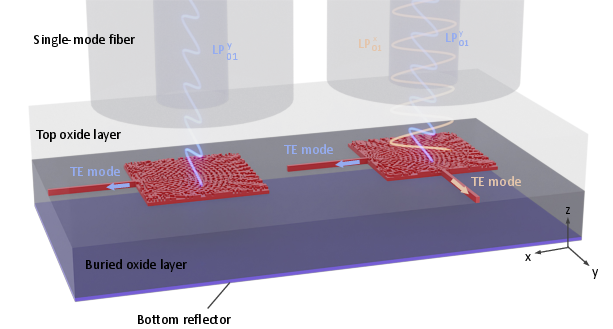
Figure 1: Schematic of the designed ultracompact topology-optimized 1D (left) and 2D grating couplers (right) incorporating a bottom reflector on the SOI platform.
The topology optimization process tailored each pixel of the design to either silicon or silicon dioxide based on their permittivity, leveraging a Python-based optimization package. This strategy harnesses 3D finite-difference time-domain simulations to maximize coupling efficiency, achieving simulated efficiencies of -0.37 dB for 1D and -0.46 dB for 2D couplers at 1550 nm.
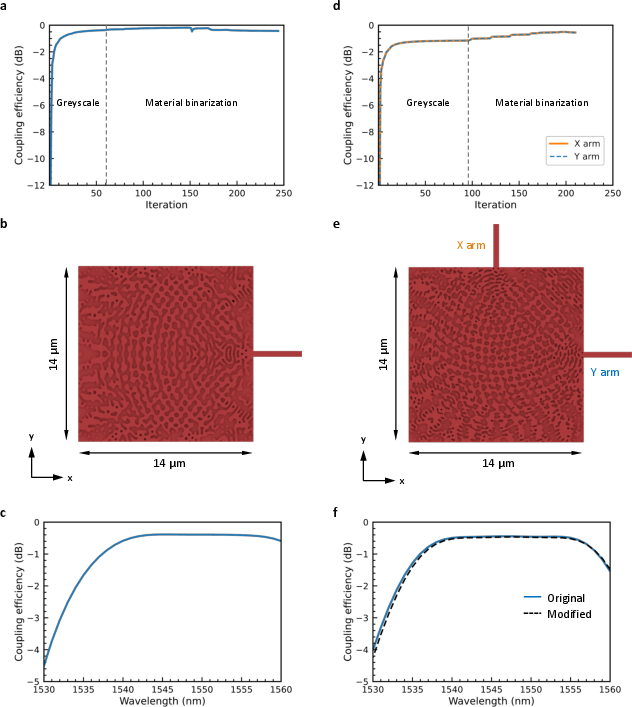
Figure 2: Simulation and optimization results of the topology-optimized grating couplers.
Fabrication and Experimental Characterization
Upon fabrication using standard CMOS processes, characterization of these grating couplers is conducted to assess their performance under operational conditions. Experimental results indicate peak measured coupling efficiencies of -0.92(1) dB for the 1D and -0.86(13) dB for the 2D coupler, demonstrating remarkable alignment with the simulated models despite minor deviations attributable to fabrication imperfections.
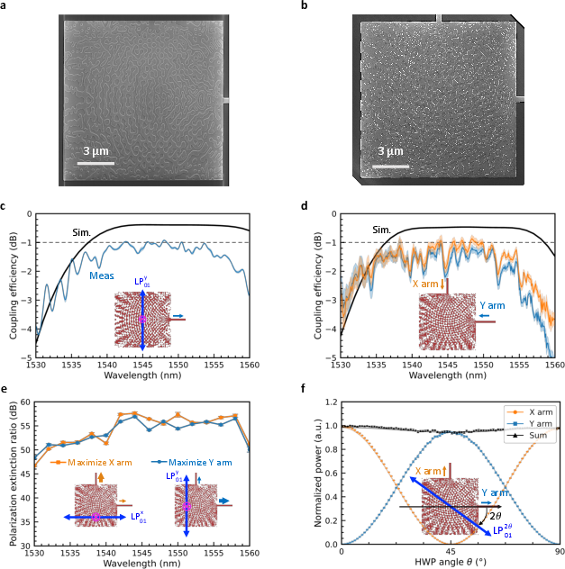
Figure 3: Fabricated topology-optimized 1D and 2D grating couplers and the experimental characterization.
The coupling efficiency profile across wavelengths from 1530 nm to 1560 nm was explored. Additionally, the 2D grating coupler registered polarization extinction ratios of 57.31 dB and 54.41 dB at 1550 nm, underlining its efficacy in polarization mode conversion.
Implications and Future Prospects
The ultracompact design and high efficiency of these grating couplers demonstrate substantial progress in the miniaturization and scalability of photonic integrated circuits. As this advance promises to bolster data transmission capacities and enhance quantum photonic applications, it is poised to spur developments in on-chip quantum state manipulation, enabling more integrated solutions for complex optical networks.
Such couplers may facilitate applications that require dense integration and minimal photon loss, including quantum key distribution and teleportation. Moreover, combining these couplers with other inverse-designed components could yield highly compact, efficient photonic circuits, furthering the integration of quantum technologies with traditional photonic systems.
Conclusion
The presented work delineates a successful application of topology optimization in the design of SOI-based grating couplers that deliver exceptional coupling efficiency. The resulting devices align well with the modern requirements of photonic systems for high-performance, high-density integration, demonstrating significant potential for both immediate practical applications and future innovations in the field.