- The paper presents a novel plasmonic logic gate design leveraging magnetoelectric light funneling to enable compact on-chip optical computing.
- It employs metal-insulator-metal waveguides and grooved metasurfaces to implement NOT, AND, and OR gates with high contrast ratios.
- The study validates performance through simulations, achieving contrast ratios up to 18.69 dB in the 1400-1450 nm telecommunication range.
Introduction
The paper discusses the design of compact plasmonic logic gates utilizing magnetoelectric light funneling within grooved metasurfaces, aimed at advancing photonic integrated circuits (PICs) in the telecommunications spectrum. The proposed architecture leverages a metal-insulator-metal (MIM) plasmonic waveguide to implement all-optical logic gates (AOLGs) such as NOT, AND, and OR. By reducing device footprint and integrating multiple logic operations within a single structure, the approach addresses challenges in traditional plasmonic structures. Operating effectively in the 1400-1450 nm range, the design promises enhanced integration into optical computing platforms.
The foundation of the device relies on light funneling in grooved metasurfaces, achieved through magnetoelectric interference (MEI) as described by Pablo et al. The metasurface uses a dielectric-filled groove acting as a Fabry-Perot resonator, enabling effective light trapping. The resonance condition is dictated by the equation (41+21m)λ=neffD, where neff is primarily influenced by the groove width and metal-dielectric interface properties.
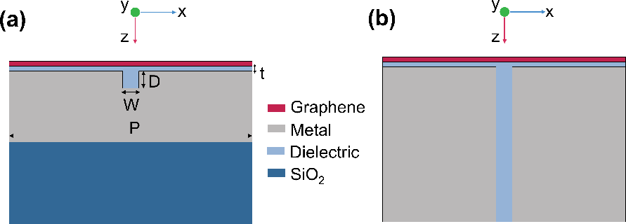
Figure 1: Light funneling in grooved metasurface involving Ag layer and dielectric groove for enhanced absorbance and transmittance.
The study utilizes a silver (Ag) Palik model with a PMMA spacer as the dielectric, emphasizing effective light funneling while exploring variations in groove dimensions. By manipulating groove parameters, absorption spectra exhibit shifts in resonant wavelengths, highlighting effective light trapping at specific configurations.
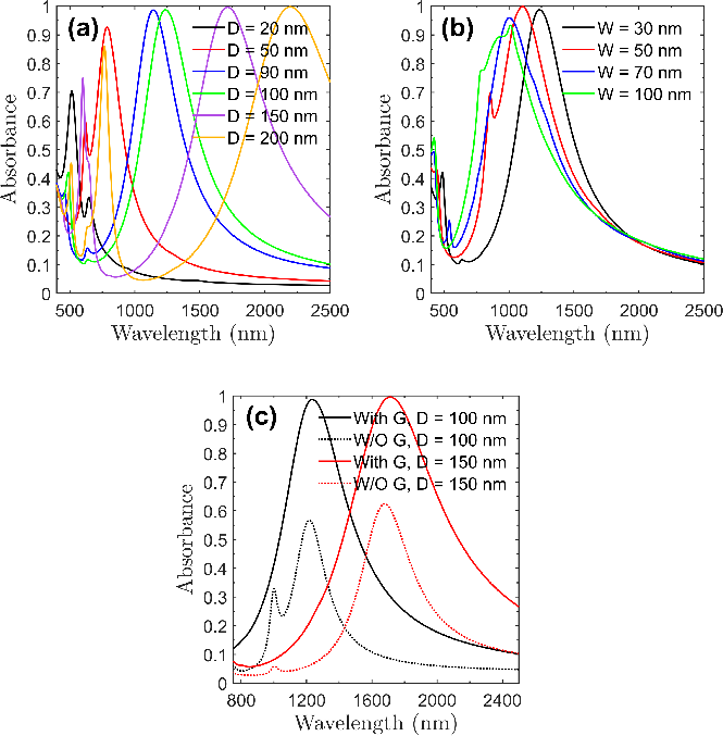
Figure 2: Absorbance spectra depicting light funneled inside for various groove depths and widths, with graphene enhancing absorbance.
Device Design and Fabrication Process
The proposed AOLG structure encompasses a three-grooved metasurface, facilitating compact implementations of NOT, AND, and OR gates. The operational principle rests on the effective refractive index neff derived from plasmonic theory, allowing precise control over resonant modes and enabling wavelength-specific operations for each logic gate.
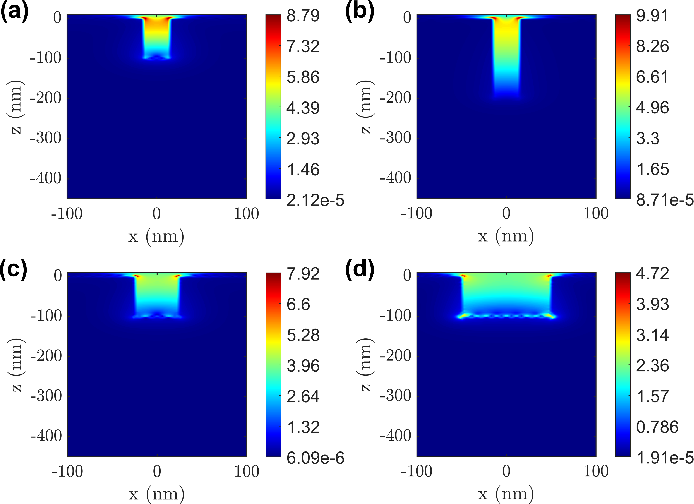
Figure 3: Variation in electric field intensity illustrating light funneling dynamics with differing groove dimensions.
The fabrication utilizes techniques like photolithography and atomic layer deposition (ALD), focusing on precise patterning and dielectric integration. The process model includes silver epitaxial layer deposition, etching, and pattern development for groove definition.
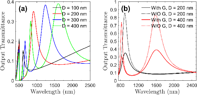
Figure 4: Transmission spectra of light funneled out, illustrating graphene's impact on transmittance with varying groove depths.
Implementation of Plasmonic Logic Gates
The design evaluates the performance of individual logic gates through simulations, assessing critical metrics like wavelength operation and contrast ratio. The finite-difference time-domain (FDTD) method aids in numerical simulations to ensure accurate representation of device behavior.
NOT Gate
For the NOT gate, the design employs a specific groove configuration to achieve a high contrast ratio of 13.8 dB, confirming effective light inversion at a wavelength of 1410 nm.
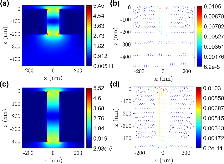
Figure 5: Electric field profile and transmission spectrum validating NOT gate functionality with distinct input configurations.
AND Gate
The AND gate design demonstrates a contrast ratio of 14.31 dB, operational at 1440 nm. The double-input configuration verifies logical conjunction with variable electric field profiles illuminating expected ON/OFF states.
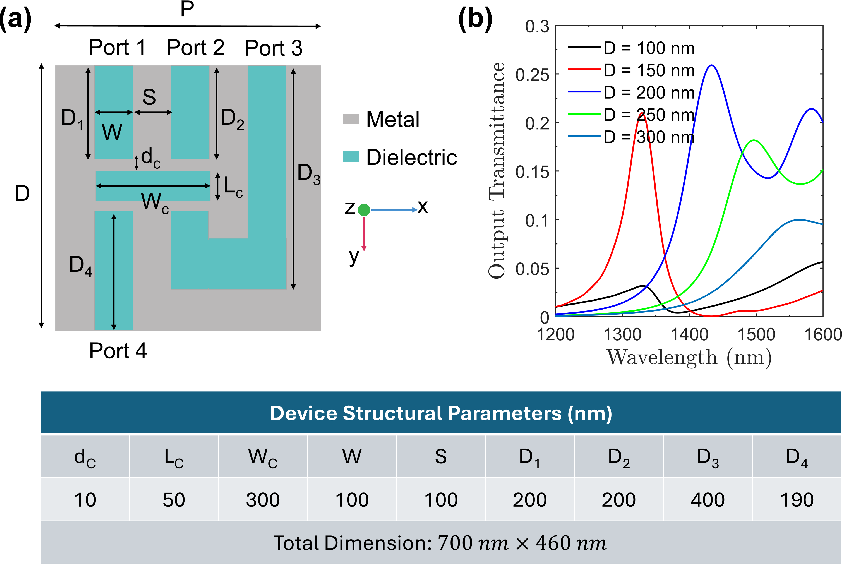
Figure 6: Electric field profiles and transmission spectrum verifying AND gate functionality and efficient logic operation.
OR Gate
The OR gate achieves a contrast ratio of 18.69 dB and operates at 1418 nm. The broad transmittance range underscores its high efficiency in logical disjunction scenarios, as evidenced by the electric field profiles and spectra analysis.
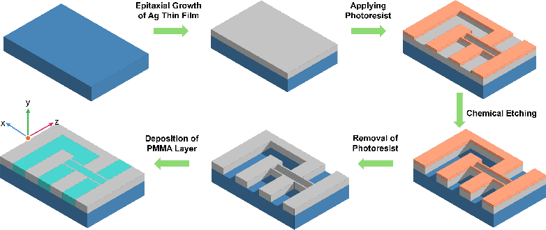
Figure 7: Transmission spectra and electric field profiles corroborating the OR gate's efficacy in optical logic gating.
Conclusion
The paper successfully demonstrates a novel approach to implement compact plasmonic logic gates through magnetoelectric light funneling, highlighting its utility in telecommunication bands. By enabling single-directional light sources with significant integration potential, the design promises to streamline and expedite optical computing in PICs. The study provides a robust framework for future explorations into miniaturized, efficient, and high-speed photonic processing systems.