- The paper presents microbenchmarks that reveal NVIDIA Blackwell's enhanced low-precision performance with extended tensor cores (FP4/FP6) and improved power efficiency.
- The study highlights that unified INT32/FP32 cores in Blackwell reduce idle cycles in mixed workloads, offering more efficient SM execution compared to Hopper.
- Memory subsystem analyses expose trade-offs in cache architectures, with Blackwell's smaller memory partitions yielding consistent latency at high instruction-level parallelism.
Dissecting the NVIDIA Blackwell Architecture with Microbenchmarks
This paper presents a microarchitectural analysis of the NVIDIA Blackwell architecture (blue chip) by employing microbenchmarks to dissect GPU performance features. The study aims to unveil key subsystems, including the memory hierarchy, SM execution pipelines, and SM sub-core units, with a focus on the 5th generation tensor cores supporting FP4 and FP6 precisions. By comparing the Blackwell architecture with the preceding Hopper architecture (GH100 chip), the paper elucidates generational improvements, performance regressions, and the role of power efficiency under varied workloads, providing insights for application developers, compiler writers, and performance engineers.
SM and Execution Pipeline Analysis
The paper details the architecture of the Streaming Multiprocessor (SM), central to both the GH100 and blue, which handles warp scheduling, instruction issue, and execution. While the fundamental SM design remains consistent, notable differences exist, as summarized in Table 1 of the paper, particularly in the distribution of execution units.
The unified INT32/FP32 cores in Blackwell improve dynamic scheduling, potentially reducing idle cycles in mixed workloads, while GH100 offers greater execution throughput and on-chip buffering for training-scale tasks. Microbenchmarks reveal that while GH100 performs better in pure INT32 and FP32 workloads, Blackwell excels in mixed instruction sequences, suggesting more efficient compute pipelines due to the unified cores.
The GH100 has 64 FP64 execution units per SM, compared to the blue with only 2. Latency measurements demonstrate that GH100 outperforms blue in FP64 computations, indicating that blue's FP64 units may primarily serve to support the instruction set, with actual calculations emulated via FP32 units or tensor cores. This insight is crucial for developers aiming for portable performance across GPUs, informing decisions on precision tradeoffs and algorithm design.
Warp Scheduler and Instruction-Level Parallelism (ILP)
(Figure 1)
Figure 1: Comparing Total Cycles vs Iterations of the blue and GH100 GPUs with INT32, FP32, and FP64 workloads.
To assess warp scheduling sensitivity and latency management under dependency chains, the paper implements a serialized dependent-instruction benchmark. As shown in Figure 1, throughput increases for the first 1-9 instructions, beyond which the pipeline behavior diverges between architectures. The GH100 tolerates short latency-bound instruction sequences better, whereas blue is optimized for more regular, high-ILP kernels. The low throughput observed for short dependent chains is attributed to inadequate ILP, which limits the GPU's ability to hide instruction latency, leading to thread stalls and underutilization of execution units.
(Figure 2)
Figure 2: Comparing Throughput vs Iterations of the blue and GH100 GPUs with INT32, FP32, and FP64 workloads.
Figure 2 shows that blue exhibits a smoother, more consistent increase in throughput compared to GH100's more irregular ramp-up.
Fifth Generation Tensor Cores and Low-Precision Arithmetic
The paper explores the fifth-generation tensor cores in Blackwell, highlighting their extended support for FP4/FP6 formats alongside FP8, which is critical for reducing memory footprint and improving throughput, particularly in inference workloads.
(Figure 3)
Figure 3: Throughput of blue and GH100 with varying precision formats and warp counts.
Table 3 of the paper indicates that GH100 lacks native support for FP4 and FP6 formats, with blue showing lower power consumption across all low-precision formats tested. As shown in Figure 3, blue has improved throughput for every precision format.
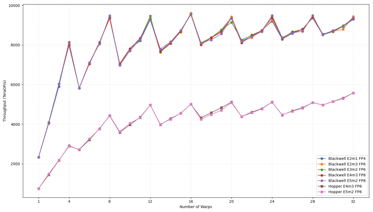
Figure 4: Latency of the blue and GH100 with varying precision formats and warp counts.
As shown in Figure 4, blue sustains consistently lower latency, especially for FP4 and FP6. Analysis of warp scaling and shared memory access reveals that Blackwell is optimized for low-precision, high-ILP workloads with clean control flow, while Hopper relies on bulk concurrency and deeper buffering.
The study examines the memory subsystems of GH100 and blue, emphasizing the importance of efficient utilization of shared memory, cache hierarchies, and global memory. Pointer-chase microbenchmarks, illustrated in Figure 5 of the paper, reveal latency spikes corresponding to cache boundaries, aligning with architectural specifications.
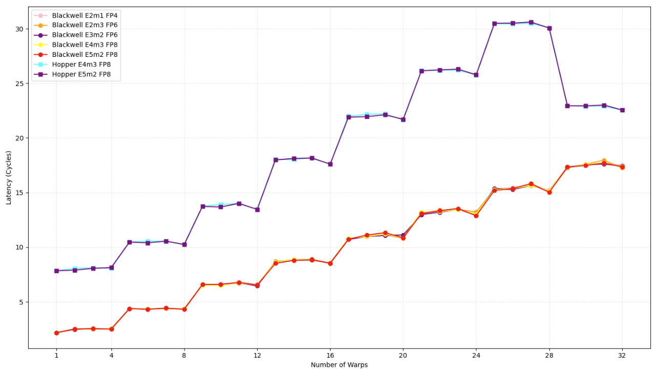
Figure 5: Latency in cycles of the memory hierarchy on the blue and GH100.
The GH100 features up to 256 KB of combined L1/shared memory per SM, whereas blue reduces this to 128 KB/SM. Shared memory latency is highly sensitive to warp count and access stride, particularly on blue, where bank conflicts scale more aggressively. As more warps access the L1 cache, blue maintains slightly lower latency from 2-11 warps, but is constrained by its smaller memory partition. The paper shows how GH100's partitioned L2 architecture is optimized for high concurrency and compute-heavy server-class workloads, while blue's unified L2 design simplifies hardware complexity and favors mixed compute-graphics use cases. Sustained transfer benchmarks indicate that GH100 achieves a peak read bandwidth of 15.8 TB/s, substantially higher than blue's 8.2 TB/s.
To evaluate real-world performance, the paper presents two case studies: Dense GEMM and Transformer Inference. The D-GEMM kernel, implemented using NVIDIA's cuBLASLt API, reveals that Hopper consistently outperforms Blackwell in runtime across nearly all matrix sizes, with Blackwell showing inconsistencies potentially due to kernel selection or scheduling issues. The Transformer inference case study, using TensorRT, shows that the Blackwell GPU benefits from a better power model, with more pronounced power reduction as precision decreases.
Conclusion
In conclusion, this paper provides a detailed microarchitectural comparison of NVIDIA's Blackwell and Hopper architectures, offering valuable insights into their respective strengths and weaknesses. The analysis underscores Blackwell's advancements in low-precision arithmetic and power efficiency, while also highlighting areas where Hopper maintains its dominance. The detailed microarchitectural analysis serves as a guide for optimizing software to effectively harness the hardware capabilities, ultimately enabling more efficient deployment of AI and HPC workloads.