GEM3D CIM General Purpose Matrix Computation Using 3D Integrated SRAM eDRAM Hybrid Compute In Memory on Memory Architecture
Abstract: With the rapid growth of deep neural networks (DNNs), compute-in-memory (CIM) has emerged as a promising energy-efficient paradigm for accelerating multiply-and-accumulate (MAC) operations. Yet, current CIM architectures are largely limited to dot-product computations and struggle to efficiently support general-purpose matrix operations, such as transpose, element-wise addition, and multiplication. This work presents a 3D-integrated, memory-on-memory SRAM-eDRAM hybrid CIM architecture, implemented in GlobalFoundries 22~nm FDSOI technology, capable of performing general matrix operations directly within the memory crossbar with 4-bit precision. By leveraging a specialized transpose-based architecture, in-memory arithmetic operations, peripheral-aware design, and 3D SRAM--eDRAM integration, the proposed architecture balances latency, energy efficiency, and compute density for general purpose matrix operations while remaining compatible with the conventional CIM dot product architectures. Overall, this memory-on-memory CIM framework generalizes CIM beyond dot products, enabling versatile matrix processing and paving the way for broader applications in AI acceleration and general-purpose high performance computing.
Paper Prompts
Sign up for free to create and run prompts on this paper using GPT-5.
Top Community Prompts
Explain it Like I'm 14
What this paper is about (big picture)
Computers spend a lot of energy and time shuttling data back and forth between memory (where data is stored) and processors (where math happens). This paper proposes a new kind of “memory that can also compute,” so some math happens right where the data already sits. Even better, it isn’t limited to just one kind of math (dot products for neural networks). It can also do other common matrix chores—like flipping a matrix (transpose), adding two matrices, and multiplying them element-by-element—directly inside the memory.
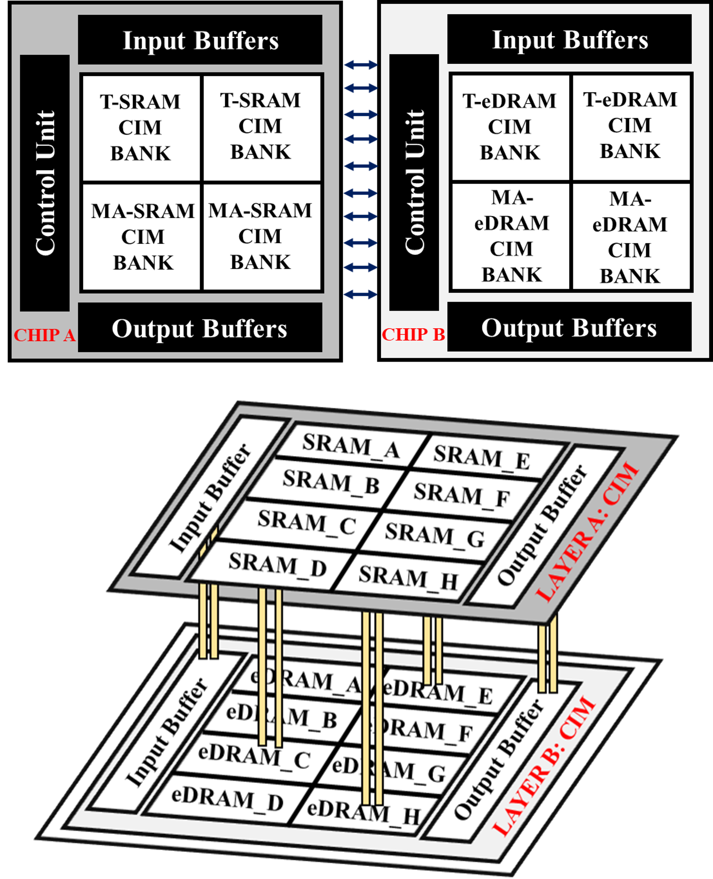
To do this, the authors stack two kinds of memory on top of each other in 3D:
- Layer A: fast and stable SRAM (like a quick-access shelf)
- Layer B: dense and energy‑efficient eDRAM (like a deep storage shelf)
Tiny vertical connections between the layers let them “talk” very quickly.
What questions the paper tries to answer
- Can we build memory that not only stores data but also performs a variety of matrix operations inside it, not just the usual dot product?
- Can this be done efficiently (fast and low energy) using real, industry-compatible chip technology?
- Can we design the memory so it plays nicely with normal digital systems, even if some of the math happens using analog signals?
How the researchers approached it (in simple terms)
Think of a library:
- Normally, you check out books (data), carry them to a study room (processor), do your work (compute), then carry them back (data movement). That’s slow and tiring.
- The authors set up study desks right between the shelves. Now you can read and write (compute) without hauling books around.
Here’s how that looks in hardware:
- 3D stacking: Two “floors” (SRAM above, eDRAM below) are connected by lots of tiny, short “elevators.” Shorter trips mean faster and more energy‑efficient communication.
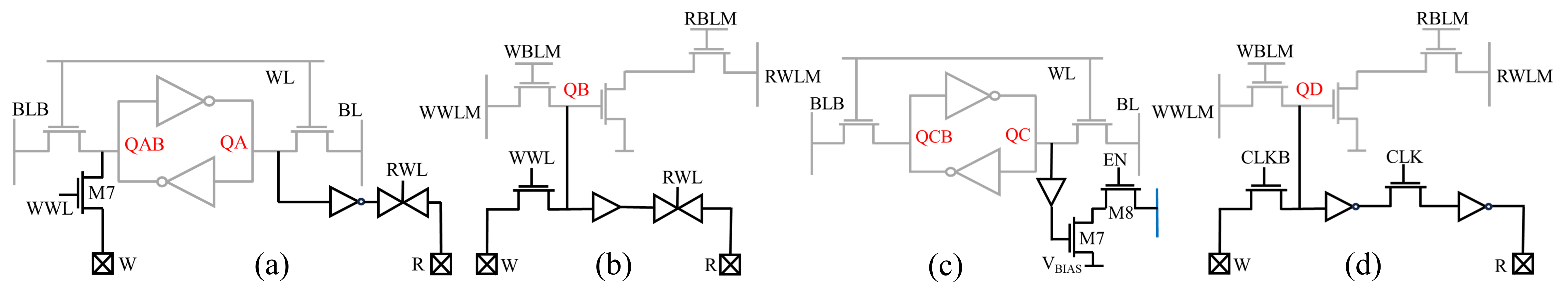
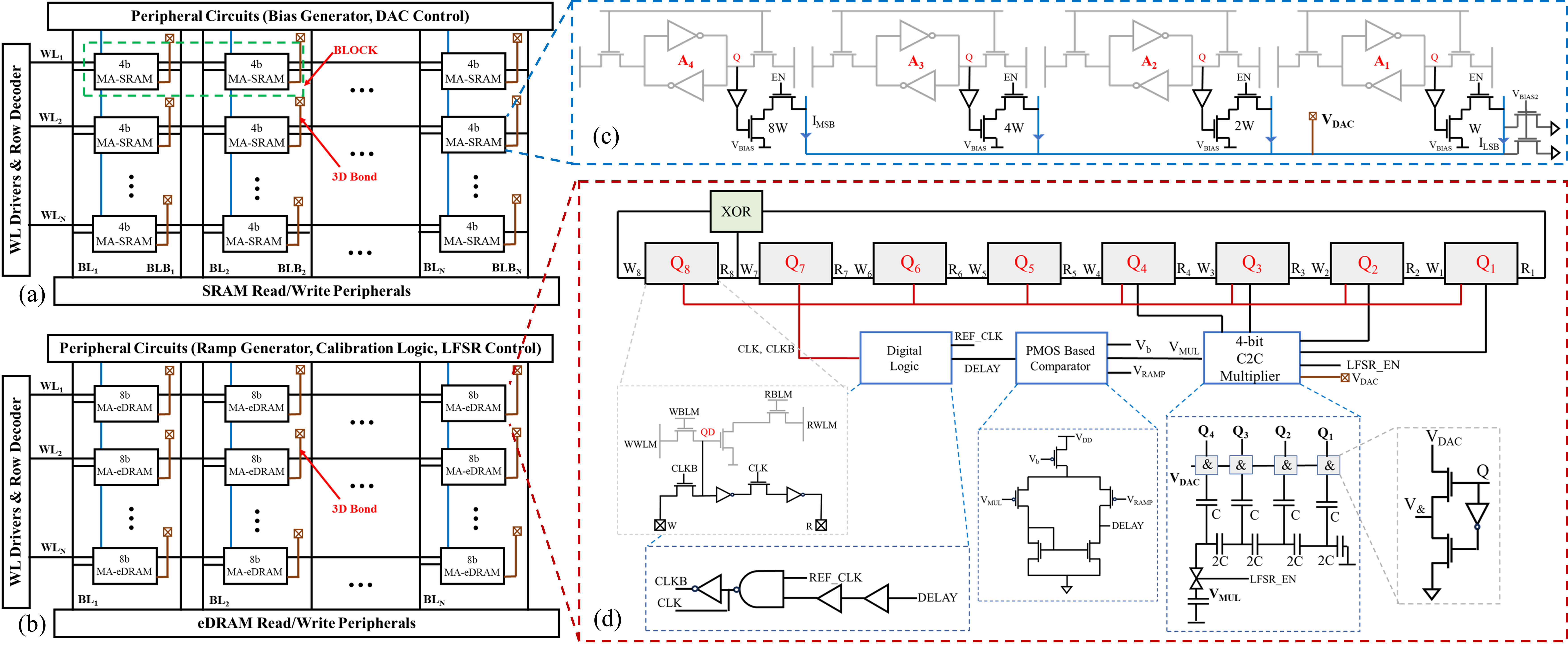
- Special memory cells:
- T‑SRAM and T‑eDRAM: These are “transposable” cells that can read and write along different directions, making it easy to swap positions of numbers for fast transpose (flipping rows and columns).
- MA‑SRAM and MA‑eDRAM: These are “math‑ready” cells for element‑wise addition and multiplication.
- Mixing digital and analog smartly:
- Digital numbers stored in memory are turned into analog voltages (like using a dimmer switch) using the SRAM (“DAC” function).
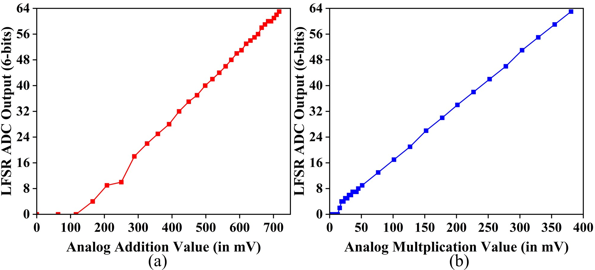
- After doing analog math (fast and compact), the result is turned back into digital using the eDRAM (an “ADC” function that uses a simple counter trick called an LFSR).
- Compatibility:
- Even though the math inside uses analog signals, both the inputs and the stored results are digital, so standard computer parts can use them.
- Still supports dot products:
- The same setup can also perform normal multiply‑and‑accumulate (MAC) operations used in neural networks.
What each main operation means (with analogies)
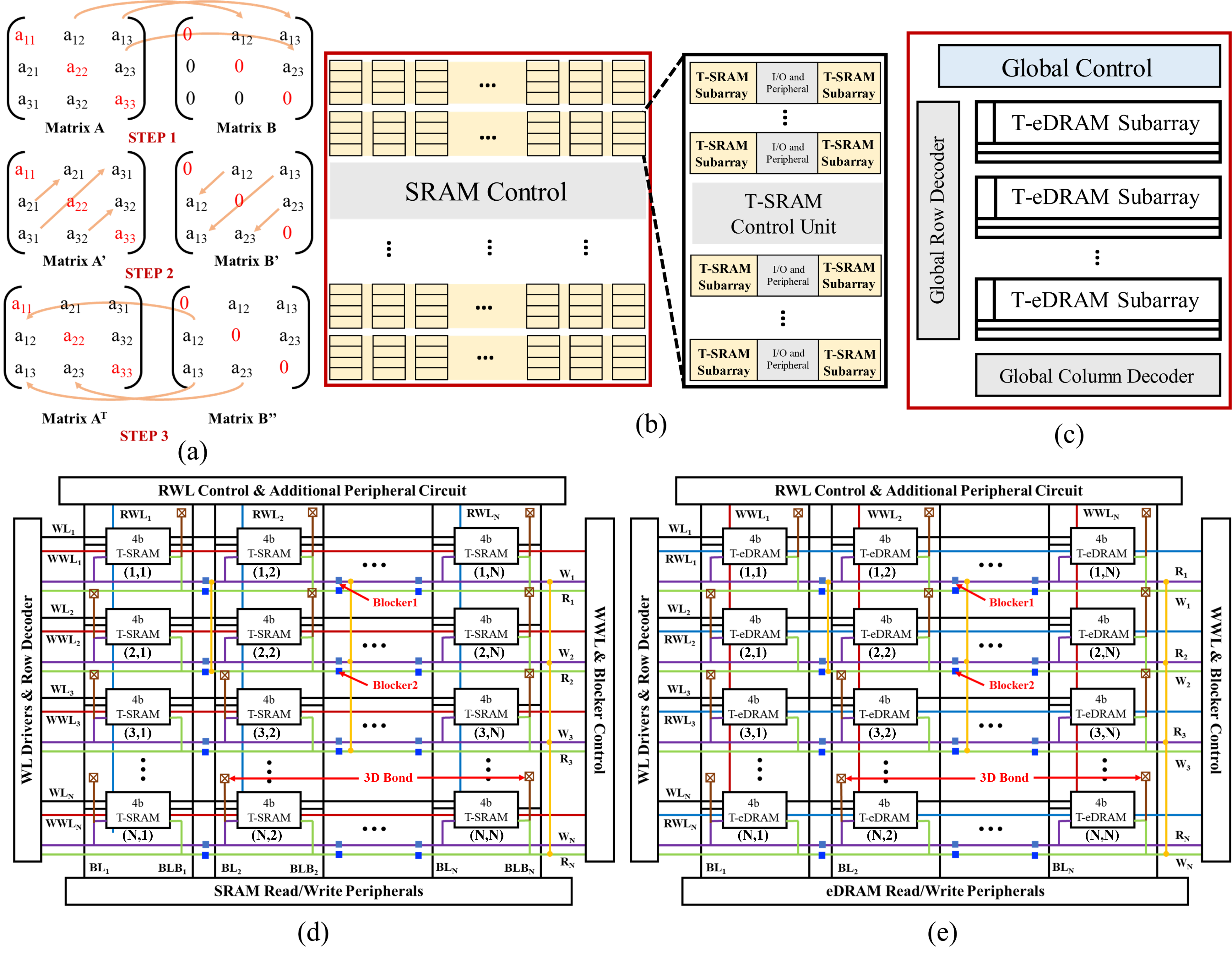
- Matrix transpose: Like flipping a spreadsheet across its main diagonal so rows become columns. The design copies elements across layers and within the same layer in a few organized steps, finishing in about N+1 steps for an N×N matrix.
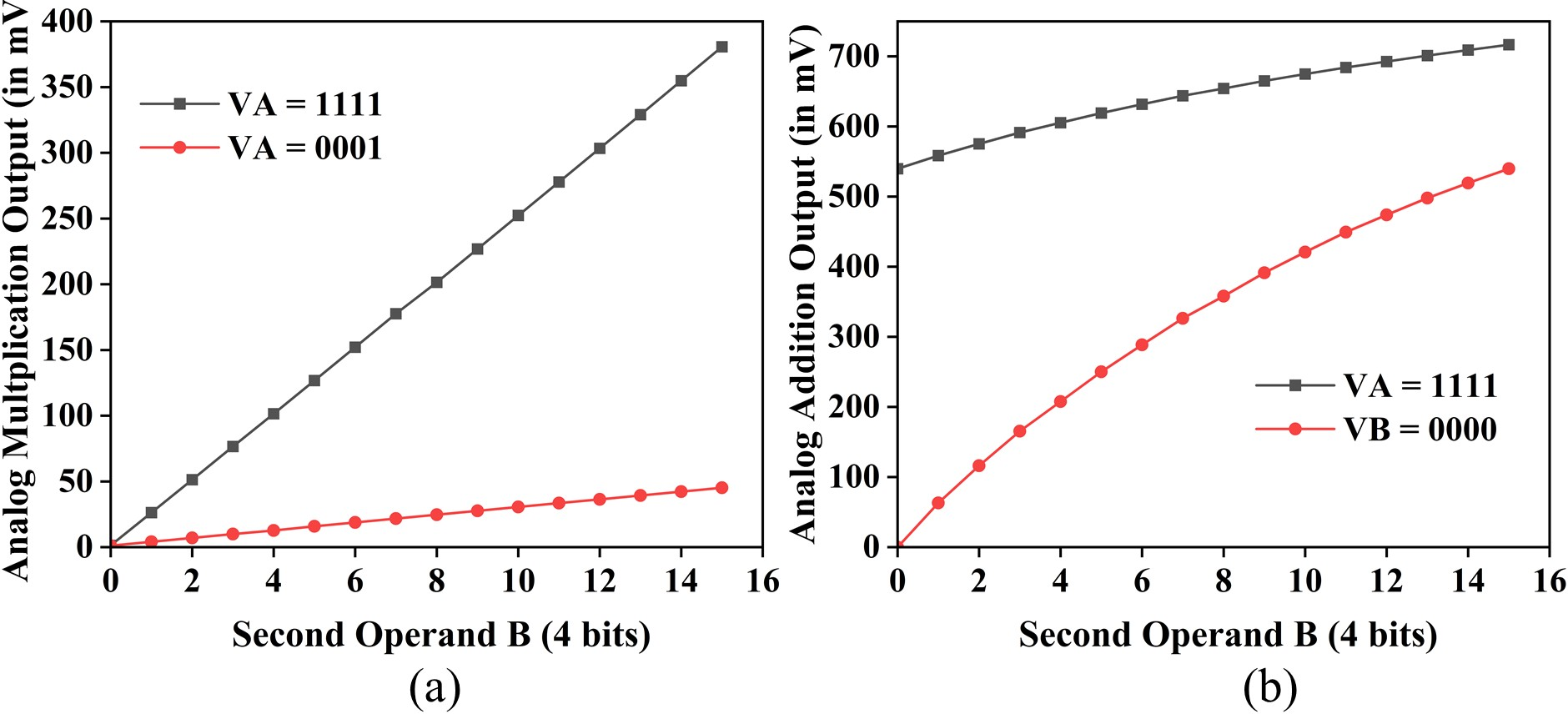
- Element‑wise addition: Add matching entries from two matrices (like adding two pictures pixel by pixel).
- Element‑wise multiplication (Hadamard product): Multiply matching entries from two matrices (like darkening or blending two images pixel by pixel).
What they built and tested
- Technology: Implemented with GlobalFoundries 22 nm FDSOI (a real, industry chip process).
- Precision: 4‑bit inputs (small numbers, enough for many AI tasks).
- Transpose engine:
- Special T‑SRAM and T‑eDRAM cells can copy and swap values in place.
- Finishes transpose in N+1 cycles (faster than doing separate read/write steps).
- Addition and multiplication engine:
- MA‑SRAM turns stored 4‑bit numbers into analog voltages (DAC).
- Simple analog circuits add or multiply those voltages.
- MA‑eDRAM converts the analog result back to digital using an LFSR‑based ADC (like timing how long it takes a ramp to catch up to a voltage).
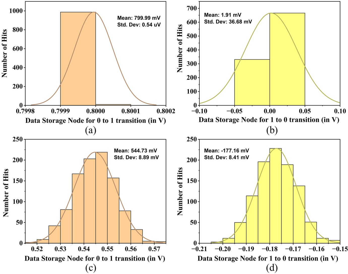
- A quick calibration step improves accuracy; the effective accuracy is around 5 bits.
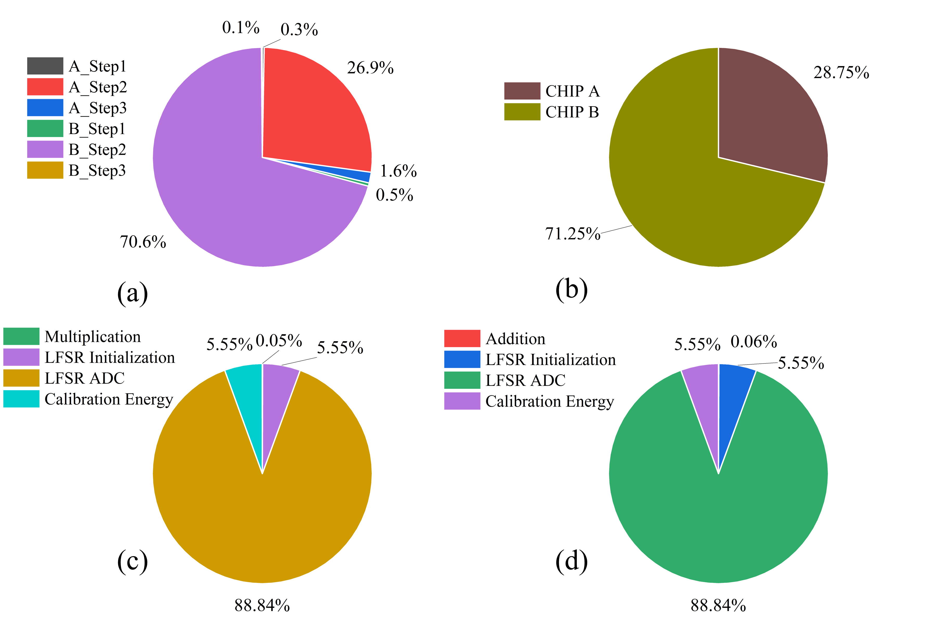
Main results and why they matter
For a 32×32 matrix (a common small test case):
- Transpose:
- Time: about 264 nanoseconds
- Energy: about 320 nanojoules
- Throughput: ~15.5 GOPS (billion operations per second)
- Energy efficiency: ~12.8 GOPS per watt
- Element‑wise multiplication (4‑bit × 4‑bit):
- Time: ~588 nanoseconds
- Energy: ~18.8 nanojoules
- Throughput: ~13.9 GOPS
- Energy efficiency: ~437 GOPS per watt
- Element‑wise addition:
- Time: ~294 nanoseconds
- Energy: ~19.0 nanojoules
- Throughput: ~27.9 GOPS
- Energy efficiency: ~432 GOPS per watt
Why this is important:
- Much less data movement: The math happens where the data lives, saving energy and time.
- More than dot products: Many algorithms (RNNs, physics simulations, masking, tensor tricks) need transpose and element‑wise ops; this system supports them directly.
- Works with standard chips: Inputs/outputs are digital and the design is foundry‑compatible, making it more practical to build and use.
- 3D stacking boosts bandwidth and density: Short, dense vertical links make the two layers act like one tightly integrated calculator.
What this could change (implications)
- Faster, greener AI hardware: Especially for tasks that use lots of matrix operations beyond just dot products.
- Broader scientific computing on memory-centric chips: Simulations and signal processing could benefit from element‑wise operations and transposes done in place.
- New chip designs: Shows a path to “memory-on-memory” compute blocks that mix analog math with digital storage using realistic manufacturing methods.
- Future directions: Improve precision, scale to larger matrices, and integrate more functions while keeping energy low.
In short, the paper shows that we can turn memory from a passive “storage closet” into an active “workbench” for many common matrix operations, all while saving energy and time—an important step for faster and more efficient AI and scientific computing.
Knowledge Gaps
Knowledge gaps, limitations, and open questions
Below is a single, consolidated list of concrete gaps and open questions that future work could address to strengthen and generalize the proposed GEM3D-CIM architecture.
- Precision and dynamic range limits: All core matrix operations are demonstrated at 4-bit inputs with an LFSR-ADC ENOB of ~4.78 bits; it remains unclear how to scale to higher bit depths (e.g., 8–12 bits) without prohibitive energy/area overhead, and how quantization/linearity errors impact end-to-end workloads.
- Inconsistent product resolution: Element-wise 4b×4b multiplication theoretically yields 8-bit products, yet the architecture reports converting to a 6-bit digital result (via 8-bit LFSR code). The rationale, precision loss, and application-level accuracy impact are not quantified.
- ADC architecture trade-offs: The choice of LFSR-based time-to-digital conversion (64-cycle) is not compared against alternatives (e.g., SAR, flash, cyclic) for speed, area, linearity, and energy across PVT; no path is provided to reduce ADC cycles or pipeline ADC for higher throughput.
- DAC/ADC non-idealities: Comprehensive INL/DNL, noise, jitter, ramp-generator distribution error, and inter-word mismatch analyses are missing; only limited Monte Carlo/linearity plots are shown without bit-error rates or failure probabilities at array scale.
- Comparator calibration robustness: The proposed per-word comparator offset calibration lacks details on storage overhead, frequency of recalibration, drift over temperature/aging, calibration convergence time, and its effect on throughput and energy at scale.
- C2C multiplier variability: Capacitor mismatch, parasitic coupling, and temperature dependence for the capacitive multiplier are not quantified; no calibration/trim strategy is proposed to maintain linearity across PVT and across large arrays.
- Analog signal distribution across tiers: The impact of monolithic inter-tier via (MIV) resistance/capacitance, crosstalk, and supply/ground noise on analog accuracy (for VDAC, VMUL, comparator inputs) is not characterized at crossbar-scale frequencies.
- eDRAM retention and refresh overhead: The retention time, refresh policies, and their energy/latency impact during compute—especially when eDRAM is used both for storage and as an LFSR counter—are not analyzed under PVT and temperature.
- Thermal management in 3D: Thermal gradients and hotspots in stacked SRAM–eDRAM, and their effects on eDRAM retention, comparator offsets, DAC/ADC linearity, and timing margins, are not modeled or experimentally validated.
- 1.8 V domain integration: The reliability (BTI/HCI), level shifters, inrush current control when switching between 0.8 V and 1.8 V, and the associated PDN/decap design and energy costs are not quantified; long-term aging and safe operating limits are not discussed.
- Energy accounting scope: Reported energy/throughput figures exclude or only partially include peripheral overheads (e.g., global ramp generator, level shifters, wordline/bitline drivers, blockers, control FSMs, inter-tier drivers). A full-chip energy budget and sensitivity to control activity are missing.
- Scalability beyond 32×32: Only a 32×32 case is parasitic-aware; scalability to larger arrays (e.g., 256×256, 1k×1k) is not validated for RC-induced delay, signal integrity, blocker resistance, read/write disturbance, and area/energy growth.
- Blocker network overheads: Transmission-gate “blockers” used for transpose introduce area, leakage, and resistance; their on/off resistance variation, timing skew, and impact on write margins and error rates across large arrays are not evaluated.
- Transpose generality: The method targets square matrices with “proper padding”; the cycle count, dataflow, and utilization for rectangular or very large matrices (with tiling across sub-arrays) remain unspecified.
- Data movement and duplication: Element-wise multiplication requires matrix B to reside in both layers (and co-location with A in Layer A). The one-time and repeated data-loading costs, bandwidth, and host–CIM I/O energy are not quantified.
- Utilization and fragmentation: Separating transpose and MA functions into dedicated sub-arrays reduces flexibility; the resulting capacity fragmentation, scheduling constraints, and system-level utilization under mixed workloads are not explored.
- Error accumulation in algorithms: No end-to-end accuracy or convergence studies (e.g., RNNs, physics kernels) quantify how analog errors from multiple transpose/add/multiply steps compound, nor how mixed-signal noise/quantization propagates through real workloads.
- Dot-product path benchmarking: While claiming compatibility with MAC, no quantitative comparison (latency/energy/accuracy) is provided versus state-of-the-art CIM dot-product arrays under identical PVT and precision assumptions.
- Throughput normalization: GOPS figures are partly estimated and use different operation definitions across works; standardized benchmarking (per-bit, per-operand, per-array) and inclusion of all control/ADC/DAC overheads are needed for fair comparisons.
- Area using logic rules: All custom bit-cells use logic design rules (not memory rules), inflating area; the feasibility, yield, and benefits of migrating to memory-rule cells or leveraging foundry SRAM/eDRAM macros are not assessed.
- Reliability and fault tolerance: There is no discussion of ECC/BISR, soft-error susceptibility (especially in eDRAM used as counters), or design-for-test strategies for monolithic 3D stacks (pre-/post-bond test, isolation of faulty tiers).
- Supply and clock distribution: Global distribution of the analog ramp, multi-GHz-equivalent timing accuracy for time-to-digital conversion, clock skew/jitter limits, and inter-tier clocking strategies are not specified.
- Control microarchitecture and programming model: The work lacks a clear ISA/runtime model, compiler mapping of high-level matrix kernels to the proposed sub-arrays, and scheduling of cross-layer operations (transpose → multiply/add → MAC) at scale.
- Concurrent operation and interference: The noise/throughput impact when transpose and arithmetic sub-arrays operate simultaneously (digital and analog activities coexisting across tiers) is uncharacterized.
- Lifetime and aging: Long-term drift of comparator offsets, DAC weights (8:4:2:1), eDRAM leakage, and MIV resistance over temperature and aging, and their maintenance/calibration strategies, remain open.
- Non-ideal line parasitics: The RC of shared R/W lines that span rows and their connection “yellow” buses is not quantified for delay, crosstalk, write disturbance, and analog corruption, especially for larger word widths and arrays.
- ADC/LFSR code mapping overhead: The LUT to convert 8-bit LFSR codes to 6-bit results imposes area/latency; its implementation details, distribution, and scalability are omitted.
- Technology portability: The design is shown in GF 22 nm FDSOI; portability to bulk FinFET nodes, different device options (e.g., no thick-oxide at advanced nodes), and changes in eDRAM availability are not discussed.
- Fabrication and yield of monolithic 3D: Practical process integration constraints (thermal budgets, inter-tier alignment tolerances, MIV yield/defects) and their impact on bit-cell yield and large-array viability are not addressed.
- Operation timing choices: The chosen cycle times (e.g., 8 ns for transpose, 3–6 ns for ADC cycles) lack justification versus worst-case PVT, array size, and noise; maximum achievable frequency and guardbands remain unclear.
- Security and isolation: With analog paths across tiers, potential side-channel leakage, data remanence in eDRAM, and cross-tenant isolation (for multi-user accelerators) are unexplored.
These gaps outline concrete directions for validating, scaling, and systematizing the proposed architecture—from circuit-level robustness and calibration, through 3D-integration and thermal/reliability considerations, to software mapping and end-to-end workload accuracy.
Practical Applications
Immediate Applications
The following use cases can be deployed now by leveraging the paper’s demonstrated 22 nm FDSOI implementation, 3D-stacked SRAM–eDRAM macros, and mixed-signal in-memory kernels (transpose, element-wise add/multiply, MAC) with 4-bit inputs and ~6-bit effective outputs via LFSR-based ADC.
- Semiconductor IP: in-situ matrix transpose macro for dataflow-heavy accelerators
- Sector: Semiconductors, AI hardware, EDA/SoC design
- What it does: Drop-in T-SRAM/T-eDRAM sub-arrays that perform in-memory transpose in N+1 cycles (vs ~2N traditionally) with digital storage and cross-tier transfer through monolithic inter-tier vias (MIVs).
- Why it matters: Reduces on-chip data movement for tensor reordering common in GEMM tiling, FFT/DCT pipelines, batched image/video transforms, and attention tensor reshapes.
- Tools/products/workflows: Macro library for T-SRAM/T-eDRAM; physical design collaterals (LEF/Lib/Verilog); RTL/firmware scheduling template for 3-step transpose across tiers; mapping pass in TVM/MLIR to fuse “transpose+compute” and minimize round-trips to cores; characterization models (latency/energy for tile sizes such as 32×32).
- Assumptions/dependencies: Foundry support for monolithic 3D or equivalent fine-pitch stacking; thermal/yield guard-banding for stacked tiers; SRAM write overdrive margin; eDRAM refresh controller; DRC with “logic rules” cell sizes (area vs density trade-off).
- Edge AI co-processor for low-precision inference
- Sector: Mobile/IoT, wearables, embedded vision/audio, robotics
- What it does: Mixed-signal, in-memory element-wise addition and Hadamard product, in-situ transpose, and conventional MAC for low-precision inference (e.g., 4-bit activations/weights, ~6-bit accumulation via LFSR ADC).
- Why it matters: Core kernels in RNN/LSTM/GRU gating (Hadamard), attention scaling/masking, residual adds, and pre/post-processing can be executed with high energy efficiency (e.g., up to ~436 GOPS/W for add/mul reported).
- Tools/products/workflows: Quantization-aware training recipes for 4-bit activations/weights; TFLite/ONNX/TensorRT custom ops for hadamard/add/transpose mapped to GEM3D-CIM; runtime that schedules DAC/ADC calibration, LFSR counting, and tier transfers; per-tile LUTs to decode LFSR codes to 6-bit values; health monitoring of PVT with in-field recalibration.
- Assumptions/dependencies: Models must tolerate 4–6 bit effective precision (ENOB ~4.8); stable analog margins (DAC signal margins, comparator offsets); periodic LFSR-based ADC calibration; 1.8 V thick-oxide devices for DAC buffers; eDRAM refresh timing integrated with compute schedule.
- Camera and ISP offload: transpose and pixel-wise ops
- Sector: Mobile imaging, AR/VR devices, autonomous sensors
- What it does: Offloads frequent transposes/reshapes between tiled color/depth planes and pixel-wise gain maps, masks, and blending (element-wise ops) directly in memory.
- Why it matters: Reduces ISP bus traffic and latency in pipelines for HDR fusion, demosaicing, and feature-map rearrangement ahead of DNN processing.
- Tools/products/workflows: ISP driver hooks to route tiles through T-SRAM/T-eDRAM sub-arrays; scheduling firmware that batches analog addition (gain/bias) and Hadamard (masking) with a single ADC pass; QC harness to validate image quality under PVT drift.
- Assumptions/dependencies: Acceptable IQ with low-precision ops in pre/post stages; careful tiling to keep within 32×32 or similar array sizes; dark-silicon budget for local comparators and ramp circuits.
- Robotics and drones: energy-efficient control and perception primitives
- Sector: Robotics, UAVs, industrial automation
- What it does: Executes element-wise gating, residual adds, and small-tile transposes in control pipelines (e.g., EKF updates, gating in RNNs for policies) and in perception backbones.
- Why it matters: Extends battery life and enables untethered operation by reducing data movement and improving GOPS/W for matrix kernels.
- Tools/products/workflows: ROS/MCU integration with a GEM3D-CIM coprocessor; microkernel library for element-wise ops and transposes; autotuner to pick tile sizes and schedule calibration cycles during idle windows.
- Assumptions/dependencies: Control/perception algorithms must be robust to low precision; environmental PVT variation management (temperature compensation).
- Academic testbed for mixed-signal CIM and 3D integration
- Sector: Academia, research labs, graduate education
- What it does: Provides a concrete, foundry-compatible platform to study algorithm–architecture co-design for CIM beyond dot products: transpose, Hadamard, addition, MAC in a single stack.
- Why it matters: Enables reproducible research on low-precision algorithms, comparator offset calibration strategies, LFSR-based ADC linearity, and monolithic 3D reliability.
- Tools/products/workflows: Open testbench RTL and SPICE decks; compiler passes for tensor tiling and operation fusion; coursework modules on CIM and 3D IC design; PVT/Monte Carlo datasets for benchmarking.
- Assumptions/dependencies: Access to GF 22 nm FDSOI PDK or a suitable academic PDK; IP licensing for educational use; lab infrastructure for analog/mixed-signal validation.
- Sustainability and procurement pilots emphasizing energy-per-op
- Sector: Public sector, enterprise IT sustainability programs
- What it does: Targets energy-intensive AI inference at the edge (e.g., smart cameras, kiosks) using in-memory compute macros to meet ESG goals.
- Why it matters: Demonstrable GOPS/W improvements on common kernels (transpose/add/mul/MAC) reduce device energy footprints.
- Tools/products/workflows: Pilot RFPs specifying energy/throughput metrics per operation (e.g., GOPS/W for element-wise ops); evaluation harnesses; runtime telemetry for energy accounting.
- Assumptions/dependencies: Availability of COTS development kits or partner SoCs embedding GEM3D-CIM macros; validation on target workloads.
Long-Term Applications
These use cases require further research, scaling, or development—especially higher precision, larger arrays, richer operation sets, and broader manufacturing availability of monolithic 3D.
- General-purpose in-memory linear algebra accelerator for HPC
- Sector: High-performance computing, scientific simulation, energy, defense
- Vision: Extend from 4–6 bit to 8–16 bit effective precision (e.g., via improved ADCs, calibration, and multi-pass accumulation), larger arrays (e.g., ≥256×256 tiles), and richer ops (reductions, scaling, fused multiply-add across tiles).
- Potential products/workflows: Memory-on-memory blades co-stacked with CPUs/GPUs to accelerate transpose-heavy kernels (blocked GEMM, FFTs, tensor permutations); compiler/runtime that orchestrates compute/refresh/calibration across hundreds of tiles; mixed-signal verification tooling at scale.
- Assumptions/dependencies: Advanced monolithic 3D processes with strong yield/thermal solutions; improved ADC linearity and offset handling; ECC for eDRAM; standardized software stacks.
- Transformer training and large-model on-device inference
- Sector: AI accelerators (datacenter and edge), mobile, AR/VR, automotive
- Vision: Scale precision and array sizes to support attention operations (QKT transposes, masking via Hadamard, residual adds) and partial training (optimizers need higher precision).
- Potential products/workflows: GEM3D-CIM backends in TVM/DeepSpeed/TensorRT; operator fusion to keep attention reorders, masking, and scaling in-memory; dynamic precision control (4–8 bits) with periodic calibration.
- Assumptions/dependencies: Quantization strategies that preserve accuracy at low precision; reliable analog compute under datacenter thermal loads; built-in self-test for continual calibration; safety features for automotive-grade silicon.
- Near-memory compute inside stacked DRAM/HBM packages
- Sector: Cloud/enterprise compute, memory vendors
- Vision: Adapt the memory-on-memory approach to high-bandwidth stacks (HBM/eDRAM-on-logic) using fine-pitch vertical interconnects to execute transposes and element-wise operations inside memory cubes.
- Potential products/workflows: HBM with “smart banklets” offering in-situ transpose and element-wise kernels exposed via CXL/PCIe extensions; host drivers and libraries that offload tensor permutations and masking to memory.
- Assumptions/dependencies: Manufacturing maturity for monolithic or hybrid bonding at HBM scale; coherence and security models for near-memory compute; standards for programming models and telemetry.
- Domain-specific signal processing appliances
- Sector: Communications (5G/6G), radar/LiDAR, audio
- Vision: In-memory acceleration of transpose- and element-wise-heavy stages in MIMO detection, beamforming weight updates, and block-based transforms with strict latency targets.
- Potential products/workflows: RF front-end companions that pre/post-process baseband tensors near memory; fixed-function pipelines using CIM macros with tunable precision; runtime that interleaves refresh, transpose, and multiply/add windows.
- Assumptions/dependencies: Enhanced precision for link budgets; deterministic timing with calibrated analog front-ends; extended operating temperature range.
- In-memory analytics for columnar databases and real-time BI
- Sector: Data analytics, finance, retail
- Vision: Offload column-wise element-wise transforms (scaling, masking, normalization steps) and frequent transposes/reshapes within memory-resident caches to reduce memory bandwidth usage.
- Potential products/workflows: Smart cache controllers with GEM3D-CIM tiles; SQL engine rewrites that map vectorized operators to in-memory kernels; correctness/precision guards for financial-grade workloads.
- Assumptions/dependencies: Precision expansion and verifiable error bounds; transactional integrity and recovery in mixed-signal paths; integration with existing cache hierarchies.
- Platformization: software, verification, and standardization
- Sector: EDA, standards bodies, compiler ecosystems
- Vision: Mature toolchains covering algorithm–architecture co-design, analog-aware compilers, mixed-signal verification at wafer scale, and standard instruction sets for in-memory ops (transpose/hadamard/add/MAC).
- Potential products/workflows: MLIR dialects for in-memory compute; analog-error models for training; ISO-style standards for monolithic 3D reliability, safety (ISO 26262), and sustainability reporting.
- Assumptions/dependencies: Broad industry alignment on abstractions; PDK access for academia/consortia; robust IP protection for mixed-signal macros.
Cross-cutting assumptions and dependencies
- Manufacturing and integration
- Availability of monolithic 3D integration (fine-pitch MIVs), thermal management for stacked tiers, and acceptable yield.
- Use of thick-oxide devices (1.8 V) for DAC buffers and reliable overdrive margins in T-SRAM write paths.
- eDRAM refresh management co-scheduled with compute and robust isolation during transpose/multiply/add operations.
- Precision, calibration, and robustness
- Current design demonstrates 4-bit inputs with ~6-bit effective outputs (LFSR ADC ENOB ~4.8 bits); scaling to ≥8 bits requires better ADCs, calibration schemes, or multi-pass aggregation.
- Comparator offsets and analog non-idealities must be calibrated (LFSR-based initial code, per-tile LUTs); PVT sensors and periodic recalibration needed for long-term stability.
- Software and workflow readiness
- Compiler/runtime support to tile tensors (e.g., 32×32), orchestrate 3-phase transposes, schedule DAC/ADC cycles, and fuse operations to amortize conversion overheads.
- Quantization-aware training and validation harnesses to ensure accuracy under low precision and analog noise.
- System integration
- Dataflow co-design to minimize host-memory shuttling; DMA engines and APIs to expose in-memory ops as first-class kernels.
- Verification and safety: mixed-signal signoff, ECC/parity for eDRAM, watchdogs for calibration drift, and fallbacks to digital paths when needed.
Glossary
Below is an alphabetical list of advanced domain-specific terms from the paper, each with a brief definition and a verbatim usage example.
- 3T eDRAM: A three-transistor embedded DRAM cell used for dense, dynamic storage with explicit refresh. "a conventional 3T eDRAM core"
- 6T SRAM: A six-transistor static RAM bit-cell used for stable, fast digital storage. "conventional 6T SRAM"
- 8T SRAM: An eight-transistor SRAM bit-cell that adds read/write decoupling or functionality (e.g., DAC). "leverages an 8T SRAM bit-cell"
- Analog to digital converter (ADC): Circuit that converts analog signals to digital codes. "analog to digital converter (ADC)"
- Bit-cell: The smallest repeatable memory storage circuit used to build arrays. "The proposed bit-cell extends the conventional 6T SRAM structure"
- Capacitive C2C multiplier: An analog multiplication technique using capacitor-to-capacitor charge redistribution. "A capacitive C2C multiplier is employed"
- Charge-domain CIM: Compute-in-memory style where computations accumulate charge on capacitors. "Charge-domain CIM offers better linearity and higher compute density and energy efficiency"
- Compute-in-memory (CIM): Performing computation directly within memory arrays to reduce data movement. "compute-in-memory (CIM) has emerged as a promising energy-efficient paradigm"
- Current-domain CIM: Compute-in-memory style where computations sum currents on wires/devices. "Current-domain CIM provides improved energy efficiency, compute density, and SNR"
- Digital-to-analog converter (DAC): Circuit that converts digital codes into analog voltages or currents. "digital-to-analog converter (DAC)"
- Differential amplifier: An amplifier that compares two input voltages to produce a differential output. "PMOS-based differential amplifier"
- Dot-product reduction: The aggregation step limiting parallelism when summing per-column partial MAC results. "performance is ultimately constrained by dot-product reduction"
- eDRAM: Embedded DRAM offering higher density than SRAM with dynamic storage behavior. "Layer B consists of eDRAM arrays"
- FDSOI: Fully-Depleted Silicon-On-Insulator CMOS technology with improved electrostatics and variability. "GlobalFoundries 22~nm FDSOI technology"
- Hadamard product: Element-wise matrix multiplication used in many algorithms. "element-wise multiplication, also known as the Hadamard product"
- Linear feedback shift register (LFSR): A shift-register with XOR feedback that cycles through pseudo-random sequences. "linear feedback shift register (LFSR) counter"
- Lookup table (LUT): A precomputed mapping used to convert codes or accelerate functions. "using a lookup table (LUT)"
- Memory crossbar: Matrix-like interconnect of memory cells enabling parallel access/compute. "within the memory crossbar"
- Memory wall: A performance limit caused by slower memory bandwidth vs processor speed. "giving rise to the well-known memory wall"
- Mixed-signal: Systems combining analog and digital circuits/processing. "mixed-signal CIM arrays"
- Monolithic 3D integration: Fabricating multiple device layers on a single wafer with fine-pitch vertical connections. "monolithic 3D integrated CIM architectures"
- Monolithic inter-tier vias (MIVs): Ultra-fine vertical vias connecting tiers in monolithic 3D stacks. "monolithic inter-tier vias (MIVs)"
- Non-volatile memories (NVMs): Memories that retain data without power (e.g., ReRAM, PCM). "non-volatile memories (NVMs)"
- ON/OFF conductance ratio: The contrast between a device’s conductive and non-conductive states. "reduced ON/OFF conductance ratio"
- Overdriven: Driving a control line above nominal supply to improve write/drive strength. "WWL lines (overdriven) are activated"
- Parasitic-aware simulations: Circuit simulations that include extracted parasitic resistances/capacitances. "parasitic-aware simulations"
- Process corners: Representative variations of manufacturing parameters used to verify robustness. "across different process corners"
- Process Design Kit (PDK): Foundry-provided models, rules, and files enabling technology-accurate design. "GlobalFoundries 22\,nm PDK"
- PVT variations: Variations in Process, supply Voltage, and Temperature affecting circuit behavior. "essential for reliable transpose operations under PVT variations"
- Ramp generator: A circuit producing a time-varying ramp voltage for time-encoding analog values. "a globally shared ramp generator"
- Read word-line (RWL): Control line that enables reading data from a memory row. "read word-lines (RWL)"
- Signal-to-noise ratio (SNR): Measure comparing signal strength to background noise level. "signal-to-noise ratio (SNR)"
- Thick-oxide devices: Transistors with thicker gate oxide for higher-voltage operation. "thick-oxide devices capable of high-voltage operation"
- Transmission gate (TG): A bidirectional CMOS switch used for low-resistance signal gating. "transmission gate (TG)"
- TSV-based: Using through-silicon vias for vertical chip stacking/interconnect. "TSV-based or flip-chip bonding approaches"
- Write word-line (WWL): Control line that enables writing data into a memory row. "write word-lines (WWL)"
Collections
Sign up for free to add this paper to one or more collections.